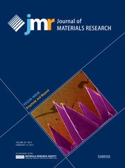
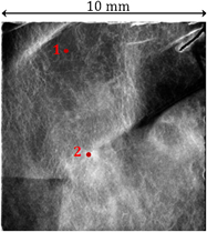
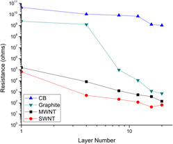
Cover: FIG. 7(a). SEM image of three CNT films stacked together. [S. Fairchild, J. Bulmer, M. Sparkes, J. Boeckl, M. Cahay, T. Back, P.T. Murray, G. Gruen, M. Lange, N.P. Lockwood, F. Orozco, W. O’Neill, C. Paukner, and K.K.K. Koziol: Field emission from laser cut CNT fibers and films. p. 392.
Graphene and Beyond
INTRODUCTION
-
- Published online by Cambridge University Press:
- 14 February 2014, pp. 297-298
-
- Article
- Export citation
Invited Reviews
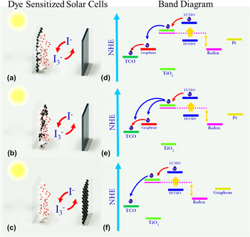
Graphene synthesis and application for solar cells
-
- Published online by Cambridge University Press:
- 15 January 2014, pp. 299-319
-
- Article
-
- You have access
- HTML
- Export citation
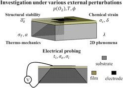
Complex oxide nanomembranes for energy conversion and storage: A review
-
- Published online by Cambridge University Press:
- 07 November 2013, pp. 320-337
-
- Article
- Export citation
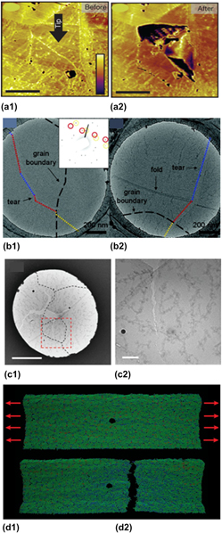
Characterizing mechanical behavior of atomically thin films: A review
-
- Published online by Cambridge University Press:
- 02 January 2014, pp. 338-347
-
- Article
- Export citation
Invited Paper
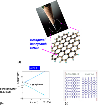
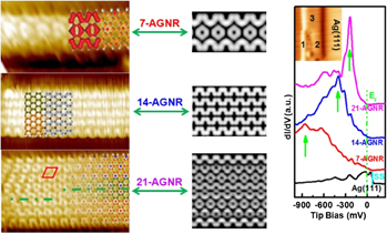
Two-dimensional layered materials: Structure, properties, and prospects for device applications
-
- Published online by Cambridge University Press:
- 14 February 2014, pp. 348-361
-
- Article
- Export citation
Invited Feature Paper
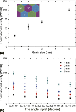
Characterizing phonon thermal conduction in polycrystalline graphene
-
- Published online by Cambridge University Press:
- 10 January 2014, pp. 362-372
-
- Article
- Export citation
Invited Papers
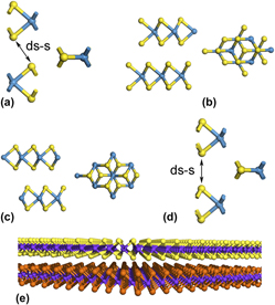
Bilayers of transition metal dichalcogenides: Different stackings and heterostructures
-
- Published online by Cambridge University Press:
- 16 October 2013, pp. 373-382
-
- Article
- Export citation
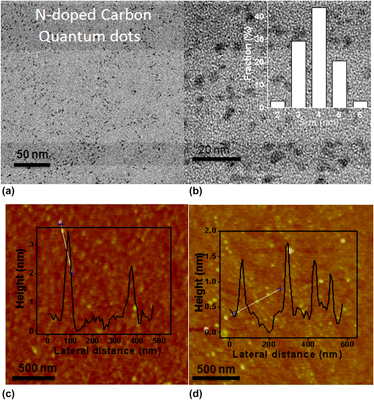
New methods of synthesis and varied properties of carbon quantum dots with high nitrogen content
-
- Published online by Cambridge University Press:
- 05 November 2013, pp. 383-391
-
- Article
- Export citation
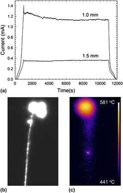
Field emission from laser cut CNT fibers and films
-
- Published online by Cambridge University Press:
- 22 November 2013, pp. 392-402
-
- Article
- Export citation
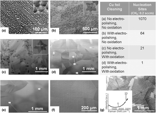
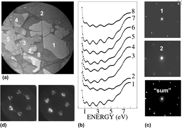
Copper oxide as a “self-cleaning” substrate for graphene growth
-
- Published online by Cambridge University Press:
- 29 January 2014, pp. 403-409
-
- Article
- Export citation
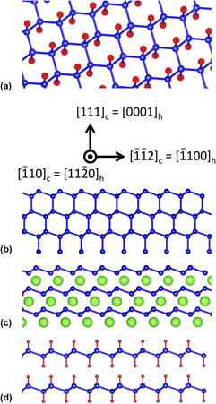
Epitaxial co-deposition growth of CaGe2 films by molecular beam epitaxy for large area germanane
-
- Published online by Cambridge University Press:
- 27 January 2014, pp. 410-416
-
- Article
- Export citation
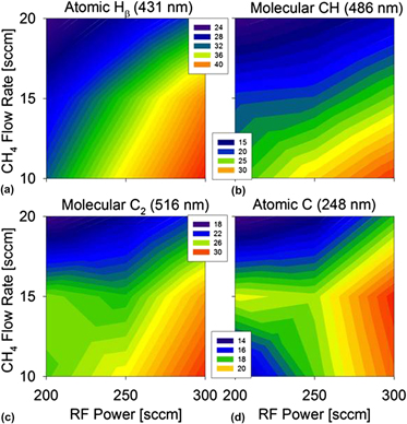
Vertical graphene by plasma-enhanced chemical vapor deposition: Correlation of plasma conditions and growth characteristics
-
- Published online by Cambridge University Press:
- 23 October 2013, pp. 417-425
-
- Article
- Export citation
Properties of epitaxial graphene grown on C-face SiC compared to Si-face
-
- Published online by Cambridge University Press:
- 23 September 2013, pp. 426-438
-
- Article
- Export citation
High-resolution x-ray analysis of graphene grown on 4H–SiC (000
 $\bar 1$) at low pressures
-
- Published online by Cambridge University Press:
- 21 November 2013, pp. 439-446
-
- Article
- Export citation
Adsorption on epitaxial graphene on SiC(0001)
-
- Published online by Cambridge University Press:
- 11 September 2013, pp. 447-458
-
- Article
- Export citation
Articles
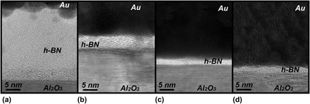
Prospects of direct growth boron nitride films as substrates for graphene electronics
-
- Published online by Cambridge University Press:
- 25 November 2013, pp. 459-471
-
- Article
- Export citation
Effect of graphitic filler size and shape on the microstructure, electrical percolation behavior and thermal properties of nanostructured multilayered carbon films deposited onto paper substrates
-
- Published online by Cambridge University Press:
- 05 December 2013, pp. 472-484
-
- Article
- Export citation
Front Cover (OFC, IFC) and matter
JMR volume 29 issue 3 Cover and Front matter
-
- Published online by Cambridge University Press:
- 14 February 2014, pp. f1-f5
-
- Article
-
- You have access
- Export citation
Back Cover (OBC, IBC) and matter
JMR volume 29 issue 3 Cover and Back matter
-
- Published online by Cambridge University Press:
- 14 February 2014, pp. b1-b2
-
- Article
-
- You have access
- Export citation

