Hostname: page-component-cd9895bd7-jkksz Total loading time: 0 Render date: 2024-12-26T03:16:15.690Z Has data issue: false hasContentIssue false

Prospects of direct growth boron nitride films as substrates for graphene electronics

Published online by Cambridge University Press:  25 November 2013

Michael S. Bresnehan
Affiliation:
Department of Materials Science and Engineering, The Pennsylvania State University, University Park, Pennsylvania 16802; Electro-Optics Center, The Pennsylvania State University, University Park, Pennsylvania 16802; and Center for 2-Dimensional and Layered Materials, The Pennsylvania State University, University Park, Pennsylvania 16802
Matthew J. Hollander
Affiliation:
Center for 2-Dimensional and Layered Materials, The Pennsylvania State University, University Park, Pennsylvania 16802; and Department of Electrical Engineering, The Pennsylvania State University, University Park, Pennsylvania 16802
Maxwell Wetherington
Affiliation:
Department of Materials Science and Engineering, The Pennsylvania State University, University Park, Pennsylvania 16802; Electro-Optics Center, The Pennsylvania State University, University Park, Pennsylvania 16802; and Center for 2-Dimensional and Layered Materials, The Pennsylvania State University, University Park, Pennsylvania 16802
Ke Wang
Affiliation:
Materials Research Institute, The Pennsylvania State University, University Park, Pennsylvania 16802
Takahira Miyagi
Affiliation:
Department of Materials Science and Engineering, The Pennsylvania State University, University Park, Pennsylvania 16802; and Materials Research Institute, The Pennsylvania State University, University Park, Pennsylvania 16802
Gregory Pastir
Affiliation:
Electro-Optics Center, The Pennsylvania State University, University Park, Pennsylvania 16802
David W. Snyder
Affiliation:
Electro-Optics Center, The Pennsylvania State University, University Park, Pennsylvania 16802; and Department of Chemical Engineering; The Pennsylvania State University, University Park, Pennsylvania 16802
Jamie J. Gengler
Affiliation:
Materials and Manufacturing Directorate, Air Force Research Laboratory, WPAFB, Ohio 45433; and Spectral Energies, LLC, Dayton, Ohio 45431
Andrey A. Voevodin
Affiliation:
Materials and Manufacturing Directorate, Air Force Research Laboratory, WPAFB, Ohio 45433
William C. Mitchel
Affiliation:
Materials and Manufacturing Directorate, Air Force Research Laboratory, WPAFB, Ohio 45433
Joshua A. Robinson*
Affiliation:
Department of Materials Science and Engineering, The Pennsylvania State University, University Park, Pennsylvania 16802; and Center for 2-Dimensional and Layered Materials, The Pennsylvania State University, University Park, Pennsylvania 16802
*
a)Address all correspondence to this author. e-mail: [email protected]
Get access

Abstract

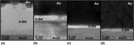
We present a route for direct growth of boron nitride via a polyborazylene to h-BN conversion process. This two-step growth process ultimately leads to a >25x reduction in the root-mean-square surface roughness of h-BN films when compared to a high temperature growth on Al2O3(0001) and Si(111) substrates. Additionally, the stoichiometry is shown to be highly dependent on the initial polyborazylene deposition temperature. Importantly, chemical vapor deposition (CVD) graphene transferred to direct-grown boron nitride films on Al2O3 at 400 °C results in a >1.5x and >2.5x improvement in mobility compared to CVD graphene transferred to Al2O3 and SiO2 substrates, respectively, which is attributed to the combined reduction of remote charged impurity scattering and surface roughness scattering. Simulation of mobility versus carrier concentration confirms the importance of limiting the introduction of charged impurities in the h-BN film and highlights the importance of these results in producing optimized h-BN substrates for high performance graphene and TMD devices.

Type
Articles
Copyright
Copyright © Materials Research Society 2013 

Access options

Get access to the full version of this content by using one of the access options below. (Log in options will check for institutional or personal access. Content may require purchase if you do not have access.)

References

REFERENCES

Dean, C.R., Young, A.F., Meric, I., Lee, C., Wang, L., Sorgenfrei, S., Watanabe, K., Taniguchi, T., Kim, P., Shepard, K.L., and Honne, J.: Boron nitride substrates for high-quality graphene electronics. Nat. Nanotechnol. 5, 722726 (2010).CrossRefGoogle ScholarPubMed
Kim, E., Yu, T., Sang Song, E., and Yu, D.: Chemical vapor deposition-assembled graphene field-effect transistor on hexagonal boron nitride. App. Phys. Lett. 98, 262103 (2011).CrossRefGoogle Scholar
Gannett, W., Regan, W., Watanabe, K., Taniguchi, T., Crommie, M.F., and Zettl, A.: Boron nitride substrates for high mobility chemical vapor deposited graphene. App. Phys. Lett. 98, 242105 (2011).CrossRefGoogle Scholar
Wang, H., Taychatanapat, T., Hsu, A., Watanabe, K., Taniguchi, T., Jarillo-Herrero, P., and Palacios, T.: BN/Graphene/BN transistors for RF applications. IEEE Electron Device Lett. 32(9), 12091211 (2011).CrossRefGoogle Scholar
Lee, K.H., Shin, H., Lee, J., Lee, I., Kim, G., Choi, J., and Kim, S.: Large-scale synthesis of high-quality hexagonal boron nitride nanosheets for large-area graphene electronics. Nano Lett. 12(2), 714718 (2012).CrossRefGoogle ScholarPubMed
Nag, A., Raidongia, K., Hembram, K.P.S.S., Datta, R., Waghmare, U.V., and Rao, C.N.R.: Graphene analogues of BN: Novel synthesis and properties. ACS Nano 4(3), 15391544 (2010).CrossRefGoogle ScholarPubMed
Bresnehan, M.S., Hollander, M.J., Wetherington, M., LaBella, M., Trumbull, K.A., Cavalero, R., Snyder, D.W., and Robinson, J.A.: Integration of hexagonal boron nitride with quasi-freestanding epitaxial graphene: Toward wafer-scale, high-performance devices. ACS Nano 6(6), 52345241 (2012).CrossRefGoogle ScholarPubMed
Hollander, M.J., Agrawal, A., Bresnehan, M.S., LaBella, M., Trumbull, K.A., Cavalero, R., Snyder, D.W., Datta, S., and Robinson, J.A.: Heterogeneous integration of hexagonal boron nitride on bilayer quasi-free-standing epitaxial graphene and its impact on electrical transport properties. Phys. Status Solidi A 210(6), 10621070 (2013).CrossRefGoogle Scholar
Bresnehan, M.S., Snyder, D.W., and Robinson, J.A.: Chemical vapor deposition of ultra-thin hexagonal boron nitride films for integration with graphene and transition metal dichalcogenides. Beyond Graphene, Poster Session (2013).Google Scholar
Li, X., Cai, W., An, J., Kim, S., Nah, J., Yang, D., Piner, R., Velamakanni, A., Jung, I., Tutuc, E., Banerjee, S.K., Colombo, L., and Ruoff, R.: Large-area synthesis of high-quality and uniform graphene films on copper foils. Science 324, 13121314 (2009).CrossRefGoogle ScholarPubMed
Shi, Y., Hamsen, C., Jia, X., Kim, K.K., Reina, A., Holfmann, M., Hsu, A.L., Zhang, K., Li, H., Juang, Z., Dresselhaus, M.S., Li, L., and Kong, J.: Synthesis of few-layer hexagonal boron nitride thin film by chemical vapor deposition. Nano Lett. 10, 41344139 (2010).CrossRefGoogle ScholarPubMed
Chan, V.Z.H., Rothman, J.B., Palladino, P., Sneddon, L.G., and Composto, R.J.: Characterization of boron nitride thin films prepared from a polymer precursor. J. Mater. Res. 11(2), 373380 (1996).CrossRefGoogle Scholar
Yu, M.C. and Jang, S.M.: Using high temperature H2 anneal to recrystallize S/D and remove native oxide simultaneously. U.S. Patent No. 6 319 784 B1, November 20, 2001.Google Scholar
Petravic, M., Peter, R., Fan, L.J., Yang, Y.W., and Chen, Y.: Direct observation of defects in hexagonal boron nitride by near-edge x-ray absorption fine structure and x-ray photoemission spectroscopy. Nucl. Instrum. Methods Phys. Res., Sect. A 619, 9497 (2010).CrossRefGoogle Scholar
Guimon, C., Gonbeau, D., Pfister-Guillouzo, G., Dugne, O., Guette, A., Naslain, R., and Lahaye, M.: XPS study of BN thin films deposited by CVD on SiC plane substrates. Surf. Interface Anal. 16, 440445 (1990).CrossRefGoogle Scholar
Wagner, C.D.: Handbook of X-ray Photoelectron Spectroscopy (Perkin-elmer, Eden Prairie, MN, 1979).Google Scholar
Schild, D., Ulrich, S., Ye, J., and Stüber, M.: XPS investigations of thick, oxygen-containing cubic boron nitride coatings. Solid State Sci. 12, 19031906 (2010).CrossRefGoogle Scholar
Trehan, R., Lifshitz, Y., and Rabalais, J.W.: Auger and x-ray electron spectroscopy studies of hBN, cBN, and N+ 2 ion irradiation of boron and boron nitride. J. Vac. Sci. Technol., A 8(6), 4026 (1990).CrossRefGoogle Scholar
Goto, T. and Hirai, T.: ESCA study of amorphous CVD Si 3 N 4-BN composites. J. Mater. Sci. Lett. 7, 548550 (1988).CrossRefGoogle Scholar
Kho, J., Moon, K., Nouet, G., Ruterana, P., and Kim, D.: Boron-rich boron nitride (BN) films prepared by a single spin-coating process of a polymeric precursor. Thin Solid Films 389, 7883 (2001).CrossRefGoogle Scholar
Fazen, P.J., Remsen, E.E., Beck, J.S., Carroll, P.J., McGhie, A.R., and Sneddon, L.G.: Synthesis, properties, and ceramic conversion reactions of polyborazylene. A high-yield polymeric precursor to boron nitride. Chem. Mater. 7, 19421956 (1995).CrossRefGoogle Scholar
Bartl, A., Bohr, S., Haubner, R., and Lux, B.: A comparison of low-pressure CVD synthesis of diamond and c-BN. Int. J. Refract. Met. Hard Mater 14, 145157 (1996).CrossRefGoogle Scholar
Chubarov, M., Pederson, H., Hogberg, H., Darakchieva, V., Jensen, J., Persson, P.O.A., and Henry, A.: Epitaxial CVD growth of sp2-hybridized boron nitride using aluminum nitride as buffer layer. Phys. Status Solidi RRL 5(10–11), 397399 (2011).CrossRefGoogle Scholar
Frueh, S., Kellett, R., Mallery, C., Molter, T., Willis, W.S., King’ondu, C., and Suib, S.L.: Pyrolytic decomposition of ammonia borane to boron nitride. Inorg. Chem. 50, 783792 (2011).CrossRefGoogle ScholarPubMed
Gengler, J.J., Roy, S., Jones, J.G., and Gord, J.R.: Two-color time-domain thermoreflectance of various metal transducers with an optical parametric oscillator. Meas. Sci. Technol. 23, 055205 (2012).CrossRefGoogle Scholar
Jo, I., Pettes, M.T., Kim, J., Watanabe, K., Taniguchi, T., Yao, Z., and Shi, L.: Thermal conductivity and phonon transport in suspended few-layer hexagonal boron nitride. Nano Lett. 13(2), 550554 (2013).CrossRefGoogle ScholarPubMed
Muratore, C., Varshney, V., Gengler, J.J., Hu, J.J., Bultman, J.E., Smith, T.M., Shamberger, P.J., Qiu, B., Ruan, X., Roy, A.K., and Voevodin, A.A.: Cross-plane thermal properties of transition metal dichalcogenides. App. Phys. Lett. 102, 081604 (2013).CrossRefGoogle Scholar
Hopkins, P.E., Baraket, M., Barnat, E.V., Beechem, T.E., Kearney, S.P., Duda, J.C., Robinson, J.T., and Walton, S.G.: Manipulating thermal conductance at metal–graphene contacts via chemical functionalization. Nano Lett. 12(2), 590595 (2012).CrossRefGoogle ScholarPubMed
Lee, J.E., Ahn, G., Shim, J., Lee, Y.S., and Ryu, S.: Optical separation of mechanical strain from charge doping in graphene. Nat. Commun. 3, 1024 (2012).CrossRefGoogle ScholarPubMed
Ahn, G., Kim, H.R., Ko, T.Y., Choi, K., Watanabe, K., Taniguchi, T., Hong, B.H., and Ryu, S.: Optical probing of the electronic interaction between graphene and hexagonal boron nitride. ACS Nano 7(2), 15331541 (2013).CrossRefGoogle ScholarPubMed
Giovannetti, G., Khomyakov, P.A., Brocks, G., Kelly, P.J., and van den Brink, J.: Substrate-induced band gap in graphene on hexagonal boron nitride: Ab initio density functional calculations. Phys. Rev. B 76, 073103 (2007).CrossRefGoogle Scholar
Ni, Z., Wang, Y., Yu, T., You, Y., and Shen, Z.: Reduction of Fermi velocity in folded graphene observed by resonance Raman spectroscopy. Phys. Rev. B 77, 235403 (2008).CrossRefGoogle Scholar
Schadler, L.S. and Galiotis, C.: Fundamentals and applications of micro Raman spectroscopy to strain measurements in fibre reinforced composites. Int. Mater. Rev. 40(3), 116134 (1995).CrossRefGoogle Scholar
Das, A., Chakraborty, B., Piscanec, S., Pisana, S., Sood, A.K., and Ferrari, A.C.: Phonon renormalization in doped bilayer graphene. Phys. Rev. B 79, 155417 (2009).CrossRefGoogle Scholar
Koenig, S.P., Boddeti, N.G., Dunn, M.L., and Bunch, J.S.: Ultrastrong adhesion of graphene membranes. Nat. Nanotechnol. 6, 543546 (2011).CrossRefGoogle ScholarPubMed
Konar, A., Fang, T., and Jena, D.: Effect of high-K gate dielectrics on charge transport in graphene-based field effect transistors. Phys. Rev. B 82, 115452 (2010).CrossRefGoogle Scholar
Fang, T., Konar, A., Xing, H., and Jena, D.: High-field transport in two-dimensional graphene. Phys. Rev. B 84, 125450 (2011).CrossRefGoogle Scholar
Katsnelson, M.I. and Geim, A.K.: Electron scattering on microscopic corrugations in graphene. Philos. Trans. R. Soc. London, Ser. A 366, 195204 (2008).Google ScholarPubMed
Miao, X., Tongay, S., and Hebard, A.F.: Strain-induced suppression of weak localization in CVD-grown graphene. J. Phys. Condens. Matter 24, 475304 (2012).CrossRefGoogle ScholarPubMed
Shah, R., Mohiuddin, T.M.G., and Singh, R.N.: Giant reduction of charge carrier mobility in strained graphene. Mod. Phys. Lett. B 27, 1350021 (2013).CrossRefGoogle Scholar
Cahill, D.G.: Analysis of heat flow in layered structures for time-domain thermoreflectance. Rev. Sci. Instrum. 75(12), 5119 (2004).CrossRefGoogle Scholar