Articles
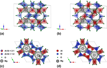
Approaching extremely low thermal conductivity by crystal structure engineering in Mg2Al4Si5O18
-
- Published online by Cambridge University Press:
- 22 December 2015, pp. 3729-3739
-
- Article
- Export citation
Invited Feature Paper
Transparent electrodes made from carbon nanotube polyelectrolytes and application to acidic environments
-
- Published online by Cambridge University Press:
- 23 June 2015, pp. 2009-2017
-
- Article
- Export citation
Articles
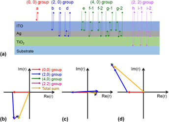
Flexible and transparent TiO2/Ag/ITO multilayer electrodes on PET substrates for organic photonic devices
-
- Published online by Cambridge University Press:
- 28 April 2015, pp. 1593-1598
-
- Article
- Export citation
Soft Nanomaterials
Introduction
-
- Published online by Cambridge University Press:
- 15 January 2015, p. 1
-
- Article
- Export citation
Articles
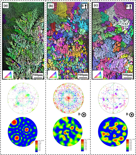
Effect of a high axial magnetic field on the structure of directionally solidified Al–Si alloys
-
- Published online by Cambridge University Press:
- 17 March 2015, pp. 1043-1055
-
- Article
- Export citation
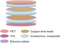
A multilayered flexible piezoresistive sensor for wide-ranged pressure measurement based on CNTs/CB/SR composite
-
- Published online by Cambridge University Press:
- 05 June 2015, pp. 1869-1875
-
- Article
- Export citation
Characterization and Modeling of Radiation Damage on Materials: State of the Art, Challenges, and Protocols
Introduction
-
- Published online by Cambridge University Press:
- 20 May 2015, p. 1157
-
- Article
- Export citation
Articles
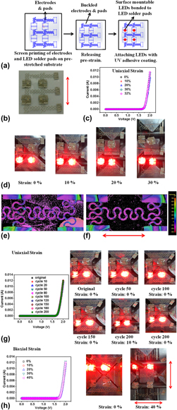
Screen printing of stretchable electrodes for large area LED matrix
-
- Published online by Cambridge University Press:
- 13 August 2015, pp. 2271-2278
-
- Article
- Export citation
Invited Feature Papers
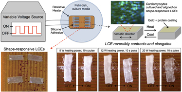
Stimuli-responsive liquid crystal elastomers for dynamic cell culture
-
- Published online by Cambridge University Press:
- 10 February 2015, pp. 453-462
-
- Article
- Export citation
Invited Feature Paper
Preparation of low-dimensional carbon material-based metal nanocomposites using a polarizable organic/water interface
-
- Published online by Cambridge University Press:
- 04 September 2015, pp. 2679-2687
-
- Article
-
- You have access
- Open access
- HTML
- Export citation
Articles
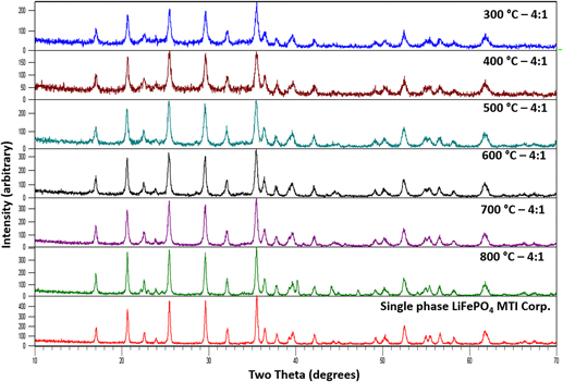
Synthesis of LiFePO4 powder by the organic–inorganic steric entrapment method
-
- Published online by Cambridge University Press:
- 27 July 2015, pp. 2133-2143
-
- Article
- Export citation
Invited Feature Papers
Porosity scaling strategies for low-k films
-
- Published online by Cambridge University Press:
- 25 November 2015, pp. 3363-3385
-
- Article
- Export citation
Invited Feature Paper
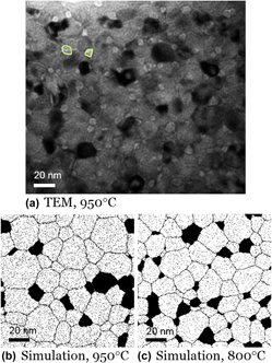
Duplex nanocrystalline alloys: Entropic nanostructure stabilization and a case study on W–Cr
-
- Published online by Cambridge University Press:
- 28 January 2015, pp. 151-163
-
- Article
-
- You have access
- HTML
- Export citation
In-situ and Operando Characterization of Materials
Introduction
-
- Published online by Cambridge University Press:
- 17 February 2015, p. 325
-
- Article
- Export citation
Nitrides and Oxynitride Materials
Introduction
-
- Published online by Cambridge University Press:
- 12 October 2015, p. 2845
-
- Article
- Export citation
Invited Feature Papers
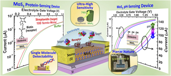
Engineered 2D nanomaterials–protein interfaces for efficient sensors
-
- Published online by Cambridge University Press:
- 20 November 2015, pp. 3565-3574
-
- Article
- Export citation
Invited Feature Paper
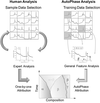
Generalized machine learning technique for automatic phase attribution in time variant high-throughput experimental studies
-
- Published online by Cambridge University Press:
- 16 April 2015, pp. 879-889
-
- Article
- Export citation
Advances in Thermoelectric Materials II
Introduction
-
- Published online by Cambridge University Press:
- 11 September 2015, p. 2517
-
- Article
- Export citation
Invited Feature Papers
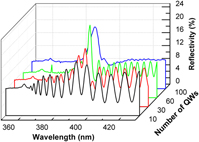
Resonant Bragg structures based on III-nitrides
-
- Published online by Cambridge University Press:
- 05 February 2015, pp. 603-608
-
- Article
- Export citation
Articles
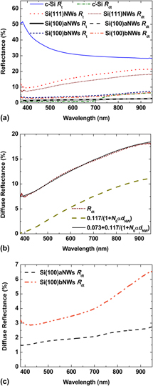
Optical properties of Si nanowires: Dependence on substrate crystallographic orientation and light polarization
-
- Published online by Cambridge University Press:
- 13 March 2015, pp. 753-760
-
- Article
- Export citation

