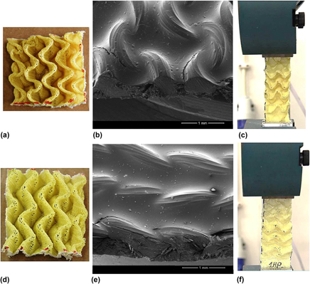
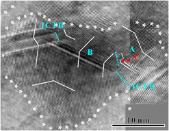
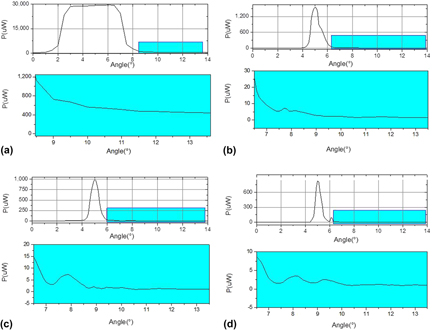
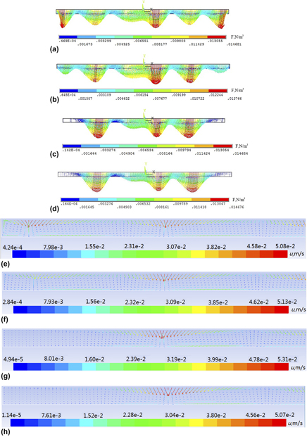
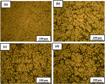
Cover: SEM micrographs. Buckling in M.F. pillars possibly due to misalignment. [F. Steffens, F. Oliveira, C. Mota, R. Fangueiro: High Performance Composite with Negative Poisson’s Ratio. p. 3477].
Invited Feature Review
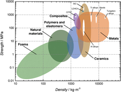
Nanocrystalline high-entropy alloys
-
- Published online by Cambridge University Press:
- 22 August 2017, pp. 3435-3444
-
- Article
- Export citation
Invited Review
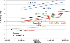
Efficiency potential and recent activities of high-efficiency solar cells
-
- Published online by Cambridge University Press:
- 22 August 2017, pp. 3445-3457
-
- Article
- Export citation
Invited Feature Paper
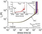
Gate dielectric reliability and instability in GaN metal-insulator-semiconductor high-electron-mobility transistors for power electronics
-
- Published online by Cambridge University Press:
- 26 September 2017, pp. 3458-3468
-
- Article
- Export citation
Articles
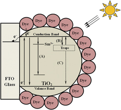
Enhanced power conversion efficiency of dye-sensitized solar cells with samarium doped TiO2 photoanodes
-
- Published online by Cambridge University Press:
- 20 September 2017, pp. 3469-3476
-
- Article
- Export citation
High-performance composite with negative Poisson’s ratio
-
- Published online by Cambridge University Press:
- 11 September 2017, pp. 3477-3484
-
- Article
- Export citation
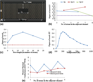
Theoretical investigation of effect of pore size and pore passivation on the thermoelectric performance of silicene nanoribbons
-
- Published online by Cambridge University Press:
- 22 August 2017, pp. 3485-3493
-
- Article
- Export citation
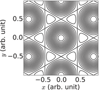
Graphene electronic structure in charge density waves
-
- Published online by Cambridge University Press:
- 17 July 2017, pp. 3494-3506
-
- Article
- Export citation
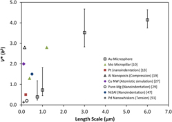
Kinetics of length-scale dependent plastic deformation of gold microspheres
-
- Published online by Cambridge University Press:
- 22 June 2017, pp. 3507-3515
-
- Article
- Export citation
Deformation-mechanism dependent stretchability of nanocrystalline gold films on flexible substrates
-
- Published online by Cambridge University Press:
- 05 September 2017, pp. 3516-3523
-
- Article
- Export citation
Invited Paper
An optical dustbin made by the subwavelength-induced super-black carbon aerogels
-
- Published online by Cambridge University Press:
- 05 September 2017, pp. 3524-3531
-
- Article
- Export citation
Articles
Optimization of traveling magnetic field for horizontal continuous casting of thin slab containing tin phosphor bronze
-
- Published online by Cambridge University Press:
- 27 June 2017, pp. 3532-3539
-
- Article
- Export citation
The influence of heat treatment on the structure and tensile properties of thin-section A356 aluminum alloy casts refined by Ti, B and Zr
-
- Published online by Cambridge University Press:
- 29 May 2017, pp. 3540-3547
-
- Article
- Export citation
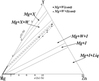
Effects of Zn content on microstructures and mechanical properties of as-cast Mg–4Y–xZn alloys
-
- Published online by Cambridge University Press:
- 07 August 2017, pp. 3548-3554
-
- Article
- Export citation
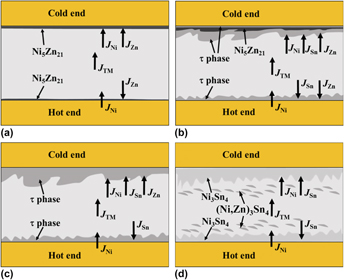
Effect of Zn content on interfacial reactions of Ni/Sn–xZn/Ni joints under temperature gradient
-
- Published online by Cambridge University Press:
- 29 August 2017, pp. 3555-3563
-
- Article
- Export citation
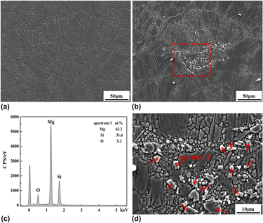
Microstructure evolution and enhanced mechanical properties of hot rolled Mg–3Al–Zn alloy with the addition of Al and Si as a eutectic alloy
-
- Published online by Cambridge University Press:
- 27 June 2017, pp. 3564-3573
-
- Article
- Export citation
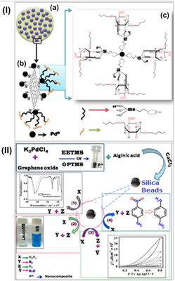
Mesoporous silica beads encapsulated with functionalized palladium nanocrystallites: Novel catalyst for selective hydrogen evolution
-
- Published online by Cambridge University Press:
- 15 June 2017, pp. 3574-3584
-
- Article
- Export citation
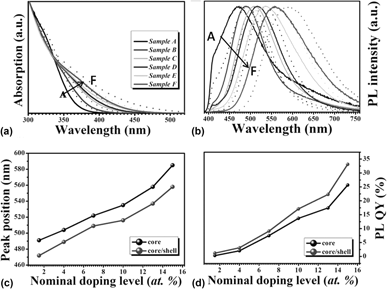
Dopant-controlled photoluminescence of Ag-doped Zn–In–S nanocrystals
-
- Published online by Cambridge University Press:
- 28 June 2017, pp. 3585-3592
-
- Article
- Export citation
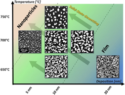
Fabrication and determination of growth regimes of various Pd NPs based on the control of deposition amount and temperature on c-plane GaN
-
- Published online by Cambridge University Press:
- 17 July 2017, pp. 3593-3604
-
- Article
- Export citation
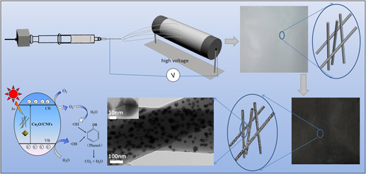
Cu2O nanoparticles supported on carbon nanofibers as a cost-effective and efficient catalyst for RhB and phenol degradation
-
- Published online by Cambridge University Press:
- 22 August 2017, pp. 3605-3615
-
- Article
- Export citation
Erratum
Effect of Zn content on interfacial reactions of Ni/Sn–xZn/Ni joints under temperature gradient – ERRATUM
-
- Published online by Cambridge University Press:
- 12 September 2017, p. 3616
-
- Article
-
- You have access
- HTML
- Export citation

