Skip to main content Accessibility help
×
Hostname: page-component-745bb68f8f-l4dxg Total loading time: 0 Render date: 2025-01-13T10:30:43.819Z Has data issue: false hasContentIssue false

8 - Probe-Based Measurement Systems

Published online by Cambridge University Press:  21 September 2017

T. Mitch Wallis
Affiliation:
National Institute of Standards and Technology, Boulder
Pavel Kabos
Affiliation:
National Institute of Standards and Technology, Boulder
Get access

Summary

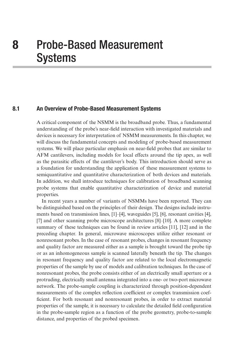
Image of the first page of this content. For PDF version, please use the ‘Save PDF’ preceeding this image.'
Type
Chapter
Information
Publisher: Cambridge University Press
Print publication year: 2017

Access options

Get access to the full version of this content by using one of the access options below. (Log in options will check for institutional or personal access. Content may require purchase if you do not have access.)

References

Fee, M., Chu, S., and Hänsch, T. W., “Scanning Electromagnetic Transmission Line Microscope with Subwavelength Resolution,” Optics Communications 69 (1989) pp. 219224.CrossRefGoogle Scholar
Steinhauer, D. E., Vlahacos, C. P., Canedy, C., Stanishevsky, A., Melngailis, R., Ramesh, R., Wellstood, F. C., and Anlage, S. M., “Imaging of Microwave Permittivity, Tunability, and Damage Recovery in (Ba,Sr)TiO3 Thin Films,” Applied Physics Letters 75 (1999) pp. 31803182.CrossRefGoogle Scholar
Tabib-Azar, M., Shoemaker, N., and Harris, S., “Nondestructive Characterization of Materials by Evanescent Microwaves,” Measurement Science and Technology 4 (1993) pp. 583590.CrossRefGoogle Scholar
Wang, M. M., Haddadi, K., Glay, D., and Lasri, T., “Compact Near Field Microwave Microscope Based on the Multi-port Technique,” Proceedings of the 40th European Microwave Conference (Paris, 2010) pp. 771774.Google Scholar
Golosovsky, M. and Davidov, D., “Novel mm-wave Near-Field Resistivity Microscope,” Applied Physics Letters 68 (1996) pp. 15791581.CrossRefGoogle Scholar
Talanov, V. V. and Schwartz, A. R., “Near-Field Scanning Microwave Microscope for Interline Capacitance Characterization of Nanoelectronics Interconnect,” IEEE Transactions on Microwave Theory and Techniques 57 (2009) pp. 12241229.CrossRefGoogle Scholar
Gao, C. and Xiang, X.-D., “Quantitative Microwave Near-Field Microscopy of Dielectric Properties,” Review of Scientific Instruments 69 (1998) pp. 38463851.CrossRefGoogle Scholar
Stranick, S. J. and Weiss, P. S., “A Versatile Microwave Frequency-Compatible Scanning Tunneling Microscope,” Review of Scientific Instruments 64 (1993) pp. 12321234.CrossRefGoogle Scholar
Tabib-Azar, M. and Wang, Y., “Design and Fabrication of Scanning Near-Field Microwave Probes Compatible with Atomic Force Microscopy to Image Embedded Microstructures,” IEEE Transactions on Microwave Theory and Techniques 52 (2004) pp. 971979.CrossRefGoogle Scholar
Lai, K., Kundhikanjana, W., Kelly, M., and Shen, Z. X., “Modeling and Characterization of Cantilever-Based Near-Field Scanning Microwave Impedance Microscope,” Review of Scientific Instruments 79 (2008) art. no. 063703.CrossRefGoogle ScholarPubMed
Rosner, B. T. and van der Weide, D. W., “High-Frequency Near-Field Microscopy,” Review of Scientific Instruments 73 (2002) pp. 25052525.CrossRefGoogle Scholar
Anlage, S. M., Talanov, V. V., and Schwartz, A. R., “Principles of Near-Field Microscope.” In Scanning Probe Microscopy (Kalinin, S. and Gruverman, A., eds.), (Springer, 2007) pp. 215253.CrossRefGoogle Scholar
Yoo, M. J., Fulton, T. A., Hess, H. F., Willet, R. L., Dunkleberger, L. N., Chichester, R. J., Pfeiffer, L. N., and West, K. W., “Scanning Single-Electron Transistor Microscopy: Imaging Individual Charges,” Science 276 (1997) pp. 579582.CrossRefGoogle ScholarPubMed
Sloggett, G. J., Barton, N. G., and Spencer, S. J., “Fringing Fields in Disc Capacitors,” Journal of Physics A: Mathematical and General 19 (1986) pp. 27252736.CrossRefGoogle Scholar
Smythe, W. R., Static and Dynamic Electricity (McGraw-Hill, 1950).Google Scholar
Kleinknecht, H. P., Sandercock, J. R., and Meier, H., “An Experimental Scanning Capacitance Microscope,” Scanning Microscopy 2 (1988) pp. 18391844.Google Scholar
Gao, C., Duewer, F., and Xiang, X.-D., “Quantitative Microwave Evanescent Microscopy,” Applied Physics Letters 75 (1999) pp. 30053007.CrossRefGoogle Scholar
Kalinin, S. V., Karapetian, E., and Kachanov, M., “Nanoelectromechanics of Piezoresponse Force Microscopy,” Physical Review B 70 (2004) art. no. 184101.CrossRefGoogle Scholar
Eliseev, E. A., Kalinin, S. V., Jesse, S., Bravina, S. L., and Morozovska, A. N., “Electromechanical Detection in Scanning Probe Microscopy: Tip Models and Materials Contrast,” Journal of Applied Physics 102 (2007) art. no. 014109.Google Scholar
Law, B. M. and Rieutord, F., “Electrostatic Forces in Atomic Force Microscopy,” Physical Review B 66 (2002) art. no. 035402.CrossRefGoogle Scholar
Sacha, G. M., Sahagun, E., and Saenz, J. J., “A Method for Calculating Capacitances and Electrostatic Forces in Atomic Force Microscopy,” Journal of Applied Physics 101 (2007) art. no. 024310.CrossRefGoogle Scholar
Sacha, G. M., “Method to Calculate Electric Fields at Very Small Tip-Sample Distances in Atomic Force Microscopy,” Applied Physics Letters 97 (2010) art. no. 033115.CrossRefGoogle Scholar
Gomez-Monivas, S., Saenz, J. J., Carminati, R., and Greffet, J. J., “Theory of Electrostatic Probe Microscopy: A Simple Perturbative Approach,” Applied Physics Letters 76 (2000) pp. 29552957.CrossRefGoogle Scholar
Hudlet, S., Saint Jeana, M., Guthmann, C., and Berger, J., “Evaluation of the Capacitive Force between an Atomic Force Microscopy Tip and a Metallic Surface,” European Physical Journal B 2 (1998) pp. 510.CrossRefGoogle Scholar
Gomila, G., Toset, J., and Fumagalli, L., “Nanoscale Capacitance Microscopy of Thin Dielectric Films,” Journal of Applied Physics 104 (2008) art. no. 024315.CrossRefGoogle Scholar
Lanyi, Š., “Effect of Tip Shape on Capacitance Determination Accuracy in Scanning Capacitance Microscopy,” Ultramicroscopy 103 (2005) pp. 221228.CrossRefGoogle ScholarPubMed
Lanyi, Š., “Shape Dependence of the Capacitance of Scanning Capacitance Microscope Probes,” Ultramicroscopy 108 (2008) pp. 712717.CrossRefGoogle ScholarPubMed
Gomila, G., Gramse, G., and Fumagalli, L., “Finite Size Effects and Analytical Modeling of Electrostatic Force Microscopy Applied to Dielectric Films,” Nanotechnology 25 (2014) art. no. 255702.CrossRefGoogle ScholarPubMed
Gramse, G., Kasper, M., Fumagalli, L., Gomila, G., Hinterdorfer, P. and Kienberger, F., “Calibrated Complex Impedance and Permittivity Measurements with Scanning Microwave Microscopy,” Nanotechnology 26 (2015) art. no. 149501.CrossRefGoogle Scholar
Naitou, Y., Yasaka, A., and Ookubo, N., “An Analytical Model for Capacitance between Probe Tip and Dielectric Film Deduced by High Frequency Electromagnetic Field Simulations,” Journal of Applied Physics 105 (2009) art. no. 044311.CrossRefGoogle Scholar
Sommerfeld, A., “Über die Ausbreitung der Wellen in der drahtlosen Telegraphie,” Annalen der Physik 28 (1909) pp. 665736.CrossRefGoogle Scholar
Sommerfeld, A., Sommerfeld, A., “Über die Ausbreitung der Wellen in der drahtlosen Telegraphie,” Annalen der Physik 81 (1926) pp. 11351153.CrossRefGoogle Scholar
Kuester, E. F. and Chang, D. C., “Evaluation of Sommerfeld Integrals Associated with Dipole Sources above Earth,” Electromagnetics Laboratory/The MIMICAD Research Center (1979) Paper 65.Google Scholar
King, R. W. P., Theory of Linear Antennas (Harvard University Press, 1956).CrossRefGoogle Scholar
Felsen, L. B. and Marcuvitz, N., Radiation and Scattering of Waves (IEEE Press, 1994).CrossRefGoogle Scholar
Wait, J. R., Electromagnetic Waves in Stratified Media (IEEE Press, 1996).Google Scholar
Lindell, I. V. and Alanen, E., “Exact Image Theory for the Sommerfeld Half-Space Problem, Part I: Vertical Magnetic Dipole,” IEEE Transactions on Antennas and Propagation 32 (1984) pp. 126133.CrossRefGoogle Scholar
Lindell, I. V. and Alanen, E., “Exact Image Theory for Sommerfeld Half-Space Problem, Part II: Vertical Electric Dipole,” IEEE Transactions on Antennas and Propagation 32 (1984) pp. 841847.CrossRefGoogle Scholar
Wait, J. R., “Possible Influence of the Ionosphere on the Impedance of a Ground-Based Antenna,” Journal of Research of the National Bureau of Standards-D 66 (1962) pp. 563569.Google Scholar
Wait, J. R., “Impedance Characteristics of Electric Dipoles over a Conducting Half-Space,” Radio Science 4 (1969) p. 971.CrossRefGoogle Scholar
Alanen, E. and Lindell, I., “Impedance of Vertical Electric and Magnetic Dipole above a Dissipative Ground,” Radio Science 19 (1984) pp. 14691474.CrossRefGoogle Scholar
Vogler, L. E. and Noble, J. L., “Curves of Input Impedance Change due to Ground for Dipole Antennas,” National Bureau of Standards (1964) Monograph 72.Google Scholar
Karbassi, A., Ruf, D., Bettermann, A. D., Paulson, C. A., van der Weide, D. W., Tanbakuchi, H., and Stancliff, R., “Quantitative Scanning Near Field Microwave Microscopy for Thin Film Dielectric Constant Measurement,” Review of Scientific Instruments 79 (2008) art. no. 094706.CrossRefGoogle ScholarPubMed
Tabib-Azar, M., Pathak, P. S., Ponchak, G., and LeClair, S., “Nondestructive Superresolution Imaging of Defects and Nonuniformities in Metals, Semiconductors, Dielectrics, Composites, and Plants Using Evanescent Microwaves,” Review of Scientific Instruments 70 (1999) pp. 27832792.CrossRefGoogle Scholar
Huber, H. P., Moertelmaier, M., Wallis, T. M., Chiang, C. J., Hochleitner, M., Imtiaz, A., Oh, Y. J., Schilcher, K., Dieudonne, M., Smoliner, J., Hinterdorfer, P., Rosner, S. J., Tanbakuchi, H., Kabos, P. and Kienberger, F., “Calibrated Nanoscale Capacitance Measurements Using a Scanning Microwave Microscope,” Review of Scientific Instruments 81 (2010) art. no. 113701.CrossRefGoogle ScholarPubMed
Hoffmann, J., Wollensack, M., Zeier, M., Niegemann, J., Huber, H-P. and Kienberger, F., “A Calibration Algorithm for Near Field, Scanning Microwave Microscopes,” Proceedings of the 2012 12th IEEE International Conference on Nanotechnology (Birmingham, 2012).Google Scholar
Farina, M., Mencarelli, D., Di Donato, A., Venanzoni, G., and Morini, A., “Calibration Protocol for Broadband Near-Field Microwave Microscopy,” IEEE Transactions on Microwave Theory and Techniques 59 (2011) pp. 27692776.CrossRefGoogle Scholar
Chisum, J. D. and Popović, Z., “Performance Limitations and Measurement Analysis of a Near-Field Microwave Microscope for Nondestructive and Subsurface Detection,” IEEE Transactions on Microwave Theory and Techniques 60 (2012) pp. 26052615.CrossRefGoogle Scholar
Dargent, T., Haddadi, K., Lasri, T., Clement, N., Ducatteau, D., Legrand, B., Tanbakuchi, H., and Theron, D., “An Interferometric Scanning Microwave Microscope and Calibration Method for Sub-fF Microwave Measurements,” Review of Scientific Instruments 84 (2013) art. no. 123705.CrossRefGoogle ScholarPubMed
Farina, M., Lucesoli, A., Pietrangelo, T., di Donato, A., Fabiani, S., Venanzoni, G., Mencarelli, D., Rozzia, T. and Morinia, A., “Disentangling Time in a Near-Field Approach to Scanning Probe Microscopy,” Nanoscale 3 (2011) pp. 35893593.CrossRefGoogle Scholar
Frait, Z., Kambersky, V., Malek, Z., and Ondris, M., “Local Variations of Uniaxial Anisotropy in Thin Films,” Czechoslovak Journal of Physics 10 (1960) p. 616.CrossRefGoogle Scholar
Soohoo, R. F., Microwave Magnetics (Harper and Row, 1985).Google Scholar
Wang, R., Li, F., and Tabib-Azar, M., “Calibration Methods of a 2 GHz Evanescent Microwave Magnetic Probe for Noncontact and Nondestructive Metal Characterization for Corrosion, Defects, Conductivity, and Thickness Nonuniformities,” Review of Scientific Instruments 76 (2005) art. no. 054701.CrossRefGoogle Scholar
An, T., Ohnishi, N., Eguchi, T., Hasegawa, Y., and Kabos, P, “Local Excitation of Ferromagnetic Resonance and Its Spatially Resolved Detection with an Open-Ended Radio-Frequency Probe,” IEEE Magnetics Letters 1 (2010) art. no. 3500104.Google Scholar
Oladipo, A. O., Lucibello, A., Kasper, M., Lavdas, S., Sardi, G. M., Proietti, E., Kienberger, F., Marcelli, R., and Panoiu, N. C., “Analysis of a Transmission Mode Scanning Microwave Microscope for Subsurface Imaging at the Nanoscale,” Applied Physics Letters 105 (2014) art. no. 133112.CrossRefGoogle Scholar
Kerns, D. M., “Plane-Wave Scattering Matrix Theory of Antennas and Antenna-Antenna Interactions,” National Bureau of Standards (1981) Monograph 162.Google Scholar

Save book to Kindle

To save this book to your Kindle, first ensure [email protected] is added to your Approved Personal Document E-mail List under your Personal Document Settings on the Manage Your Content and Devices page of your Amazon account. Then enter the ‘name’ part of your Kindle email address below. Find out more about saving to your Kindle.

Note you can select to save to either the @free.kindle.com or @kindle.com variations. ‘@free.kindle.com’ emails are free but can only be saved to your device when it is connected to wi-fi. ‘@kindle.com’ emails can be delivered even when you are not connected to wi-fi, but note that service fees apply.

Find out more about the Kindle Personal Document Service.

Available formats
×

Save book to Dropbox

To save content items to your account, please confirm that you agree to abide by our usage policies. If this is the first time you use this feature, you will be asked to authorise Cambridge Core to connect with your account. Find out more about saving content to Dropbox.

Available formats
×

Save book to Google Drive

To save content items to your account, please confirm that you agree to abide by our usage policies. If this is the first time you use this feature, you will be asked to authorise Cambridge Core to connect with your account. Find out more about saving content to Google Drive.

Available formats
×