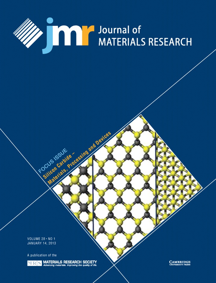
Focus Issue: Silicon Carbide – Materials, Processing and Devices
Cross-sectional and side views, respectively, of 3C-SiC NWs cut along <001> (left), <011> (middle), and <111> (right). The wire axis is indicated on the side view (vertical arrow). Carbon and silicon atoms are indicated by black and yellow balls, respectively.Orientations and locations of dimers for each of the wire geometries are different and they are indicated in the figure by drawing circular loops around C-C dimers and Si-Si dimers, respectively. In the case of <011>-oriented NWs with hexagonal morphology (Hexagon-1), the dimers are oriented perpendicular to the nanowire axis (side view); in the case of <111>-oriented NWs with hexagonal morphology, the dimers are located at the corners of the hexagon (top view). [M. Yu, C.S. Jayanthi, and S.Y. Wu. Size, shape, and orientation-dependent properties of SiC nanowires of selected bulk polytypes. p. 57].
Front Cover (OFC, IFC) and matter
JMR volume 28 issue 1 Cover and Front matter
-
- Published online by Cambridge University Press:
- 11 January 2013, pp. f1-f5
-
- Article
-
- You have access
- Export citation
Back Cover (OBC, IBC) and matter
JMR volume 28 issue 1 Cover and Back matter
-
- Published online by Cambridge University Press:
- 11 January 2013, pp. b1-b4
-
- Article
-
- You have access
- Export citation

