Hostname: page-component-78c5997874-ndw9j Total loading time: 0 Render date: 2024-11-15T13:24:42.577Z Has data issue: false hasContentIssue false

Polarity of GaN with polar {0001} and semipolar ${\left\{ {{\bf10} {\bar {\bf 1}\bf1} \right\}}}$, ${\left\{ {{\bf20}\bar {\bf 2}\bf1} \right\}}}$, ${\left\{ {{\bf11}\bar {\bf 2}\bf2} \right\}}}$ orientations by x-ray photoelectron diffraction

Published online by Cambridge University Press:  05 June 2015
Oleksandr Romanyuk*
Affiliation:
Institute of Physics, Academy of Sciences of the Czech Republic, Cukrovarnicka 10, 162 53 Prague, Czech Republic
Petr Jiříček
Affiliation:
Institute of Physics, Academy of Sciences of the Czech Republic, Cukrovarnicka 10, 162 53 Prague, Czech Republic
Tania Paskova
Affiliation:
Department of Electrical and Computer Engineering, North Carolina State University, Raleigh, North Carolina 27606, USA
Igor Bartoš
Affiliation:
Institute of Physics, Academy of Sciences of the Czech Republic, Cukrovarnicka 10, 162 53 Prague, Czech Republic
*
a)Address all correspondence to this author. e-mail: [email protected]
Get access

Abstract

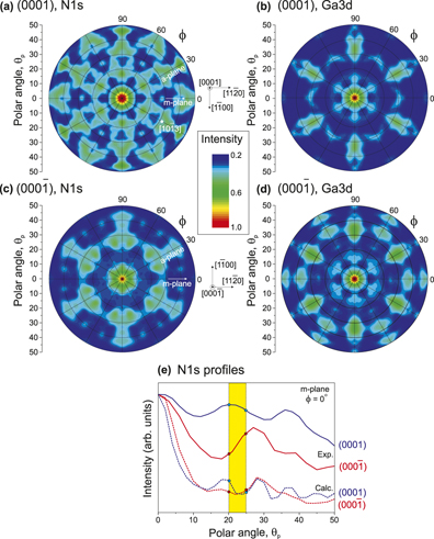
A fast and nondestructive method for polarity determination of wurtzite GaN crystals based on x-ray photoelectron diffraction (XPD) has been demonstrated. Photoelectron emission from N 1s core level excited by Mg Kα source was found sufficient for the polarity determination of GaN crystals. XPD polar plots from polar GaN {0001} and semipolar GaN$\{ 10\bar 11\}$, $\left\{ {20\bar 21} \right\}$, $\left\{ {11\bar 22} \right\}$ crystals have been analyzed. Due to dominant electron forward scattering along N–Ga directions, photoelectron intensities either increase or decrease within a relatively narrow emission polar angle range. The slopes of polar plots are found noticeably different in the polar angle range of 20°–25° for (0001) or $\left( {000\bar 1} \right)$ crystals, respectively. The semipolar GaN substrates can be divided into two groups, depending on whether m-plane or a-plane is perpendicular to the semipolar surface. It was found that the slopes of the polar plots are different in the angular range of 20°–27° for semipolar GaN$\left\{ {10\bar 11} \right\}$, 10°–22° for GaN$\left\{ {20\bar 21} \right\}$ substrates, while for the GaN$\left\{ {11\bar 22} \right\}$ semipolar planes, the slopes are different in the range of 0°–15° with respect to the surface normal.

Type
Articles
Copyright
Copyright © Materials Research Society 2015 

Access options

Get access to the full version of this content by using one of the access options below. (Log in options will check for institutional or personal access. Content may require purchase if you do not have access.)

References

REFERENCES

Huang, D., Visconti, P., Jones, K., Reshchikov, M.A., Yun, F., Baski, A.A., King, T., and Morkoc, H.: Dependence of GaN polarity on the parameters of the buffer layer grown by molecular beam epitaxy. Appl. Phys. Lett. 78, 4145 (2001).CrossRefGoogle Scholar
Cao, B., Xu, K., Seo, B.W., Arita, S., Nishida, S., Ishitani, Y., and Yoshikawa, A.: Dependences of GaN polarity on the growth temperatures of migration-enhanced-epitaxy-grown AlN in MOVPE. Phys. Status Solidi C 0, 2553 (2003).CrossRefGoogle Scholar
Hite, J.K., Garces, N.Y., Goswami, R., Mastro, M.A., Kub, F.J., and Eddy, C.R.: Selective switching of GaN polarity on Ga-polar GaN using atomic layer deposited Al2O3 . Appl. Phys. Express 7, 025502 (2014).CrossRefGoogle Scholar
Cruz, S.C., Keller, S., Mates, T.E., Mishra, U.K., and DenBaars, S.P.: Crystallographic orientation dependence of dopant and impurity incorporation in GaN films grown by metalorganic chemical vapor deposition. J. Cryst. Growth 311, 3817 (2009).CrossRefGoogle Scholar
Huang, C-Y., Hardy, M.T., Fujito, K., Feezell, D.F., Speck, J.S., DenBaars, S.P., and Nakamura, S.: Demonstration of 505 nm laser diodes using wavelength-stable semipolar $\left( {20\bar 2\bar 1} \right)$ InGaN/GaN quantum wells. Appl. Phys. Lett. 99, 241115 (2011).CrossRefGoogle Scholar
Wilkins, S., Greenough, M., Arellano, C., Paskova, T., and Ivanisevic, A.: In-situ functionalization of gallium nitride with phosphoric acid derivatives during etching. Langmuir 30, 2038 (2014).CrossRefGoogle ScholarPubMed
Speck, J. and Chichibu, S.F.: Nonpolar and semipolar group III nitride-based materials. MRS Bull. 34, 304 (2009).CrossRefGoogle Scholar
Paskova, T.: Development and prospects of nitride materials and devices with nonpolar surfaces. Phys. Status Solidi B 245, 1011 (2008).CrossRefGoogle Scholar
Durnev, M.V., Omelchenko, A.V., Yakovlev, E.V., Evstratov, I.Yu., and Karpov, S.Yu.: Indium incorporation and optical transitions in InGaN bulk materials and quantum wells with arbitrary polarity. Appl. Phys. Lett. 97, 051904 (2010).CrossRefGoogle Scholar
Akiyama, T., Yamashita, T., Nakamura, K., and Ito, T.: Stability and indium incorporation processes on In0.25Ga0.75N surfaces under growth conditions: First-principles calculations. Jpn. J. Appl. Phys. 49, 030212 (2010).CrossRefGoogle Scholar
Nishizuka, K., Funato, M., Kawakami, Y., Fujita, S., Narukawa, Y., and Mukai, T.: Efficient radiative recombination from 〈112-2〉 -oriented In x Ga1−x N multiple quantum wells fabricated by the regrowth technique. Appl. Phys. Lett. 85, 3122 (2004).CrossRefGoogle Scholar
Funato, M., Ueda, M., Kawakami, Y., Narukawa, Y., Kosugi, T., Takahashi, M., and Mukai, T.: Blue, green, and amber InGaN/GaN light-emitting diodes on semipolar $\left\{ {11\bar 22} \right\}$ GaN bulk substrates. Jpn. J. Appl. Phys. 45, L659 (2006).CrossRefGoogle Scholar
Funato, M. and Kawakami, Y.: Semipolar III nitride semiconductors: Crystal growth, device fabrication, and optical anisotropy. MRS Bull. 34, 334 (2009).CrossRefGoogle Scholar
Funato, M., Kotani, T., Kondou, T., and Kawakami, Y.: Semipolar {n-n 01} InGaN/GaN ridge quantum wells (n = 1−3) fabricated by a regrowth technique. Appl. Phys. Lett. 100, 162107 (2012).CrossRefGoogle Scholar
Scholz, F., Wunderer, T., Feneberg, M., Thonke, K., Chuvilin, A., Kaiser, U., Metzner, S., Bertram, F., and Christen, J.: GaInN-based LED structures on selectively grown semi-polar crystal facets. Phys. Status Solidi A 207, 1407 (2010).CrossRefGoogle Scholar
Scholz, F., Wunderer, T., Neubert, B., Feneberg, M., and Thonke, K.: GaN-based light-emitting diodes on selectively grown semipolar crystals facets. MRS Bull. 34, 334 (2009).CrossRefGoogle Scholar
Wunderer, T., Lipski, F., Schwaiger, S., Hertkorn, J., Wiedenmann, M., Feneberg, M., Thonke, K., and Scholz, F.: Properties of blue and green InGaN/GaN quantum well emission on structured semipolar surfaces. Jpn. J. Appl. Phys. 48, 060201 (2009).CrossRefGoogle Scholar
Tischer, I., Feneberg, M., Schirra, M., Yacoub, H., Sauer, R., Thonke, K., Wunderer, T., Scholz, F., Dieterle, L., Müller, E., and Gerthsen, D.: I 2 basal plane stacking fault in GaN: Origin of the 3.32 eV luminescence band. Phys. Rev. B 83, 035314 (2011).CrossRefGoogle Scholar
Scholz, F., Meisch, T., Caliebe, M., Schrner, S., Thonke, K., Kirste, L., Bauer, S., Lazarev, S., and Baumbach, T.: Growth and doping of semipolar GaN grown on patterned sapphire substrates. J. Cryst. Growth 405, 97 (2014).CrossRefGoogle Scholar
Meisch, T., Alimoradi-Jazi, M., Klein, M., and Scholz, F.: $\left( {20\bar 21} \right)$ MOVPE and HVPE GaN grown on 2” patterned sapphire substrates. Phys. Status Solidi C 11, 537 (2014).CrossRefGoogle Scholar
Nepal, N., Frajtag, P., Zavada, J.M., El-Masry, N.A., and Bedair, S.M.: Light emitting diodes based on sidewall m-plane epitaxy of etched GaN/sapphire templates. Phys. Status Solidi C 8, 2354 (2011).CrossRefGoogle Scholar
Frajtag, P., Nepal, N., Paskova, T., Bedair, S.M., and El-Masry, N.A.: Multifacet semipolar formation by controlling the groove depth via lateral sidewall epitaxy. J. Cryst. Growth 367, 88 (2013).CrossRefGoogle Scholar
de Mierry, P., Kriouche, N., Nemoz, M., Chenot, S., and Nataf, G.: Semipolar GaN films on patterned r-plane sapphire obtained by wet chemical etching. Appl. Phys. Lett. 96, 231918 (2010).CrossRefGoogle Scholar
Tendille, F., De Mierry, P., Vennéguès, P., Chenot, S., and Teisseire, M.: Defect reduction method in (11-22) semipolar GaN grown on patterned sapphire substrate by MOCVD: Toward heteroepitaxial semipolar GaN free of basal stacking faults. J. Cryst. Growth 404, 177 (2014).CrossRefGoogle Scholar
Zhong, H., Tyagi, A., Pfaff, N., Saito, M., Fujito, K., Speck, J.S., DenBaars, S.P., and Nakamura, S.: Enhancing the light extraction efficiency of blue semipolar (1011) nitride-based light emitting diodes through surface patterning. Jpn. J. Appl. Phys. 48, 030201 (2009).CrossRefGoogle Scholar
Enya, Y., Yoshizumi, Y., Kyono, T., Akita, K., Ueno, M., Adachi, M., Sumitomo, T., Tokuyama, S., Ikegami, T., Katayama, K., and Nakamura, T.: 531 nm Green lasing of InGaN based laser diodes on semi-polar {2021} free-standing GaN substrates. Appl. Phys. Express 2, 082101 (2009).CrossRefGoogle Scholar
Raring, J.W., Schmidt, M.C., Poblenz, C., Li, B., Chang, Y-C., Mondry, M.J., Lin, Y-D., Krames, M.R., Craig, R., Speck, J.S., DenBaars, P., and Nakamura, S.: High-performance blue and green laser diodes based on nonpolar/semipolar bulk GaN substrates. Proc. SPIE 7939, 79390Y-1 (2011).CrossRefGoogle Scholar
Seelmann-Eggebert, M., Weyher, J., Obloh, H., Zimmermann, H., Rar, A., and Porowski, S.: Polarity of (00.1) GaN epilayers grown on a (00.1) sapphire. Appl. Phys. Lett. 71, 2635 (1997).CrossRefGoogle Scholar
Hestroffer, K., Bougerol, C., Leclere, C., Renevier, H., and Daudin, B.: Polarity of GaN nanowires grown by plasma-assisted molecular beam epitaxy on Si(111). Phys. Rev. B 84, 245302 (2011).CrossRefGoogle Scholar
Fernández-Garrido, S., Kong, X., Gotschke, T., Calarco, R., Geelhaar, L., Trampert, A., and Brandt, O.: Spontaneous nucleation and growth of GaN nanowires: The fundamental role of crystal polarity. Nano Lett. 12, 6119 (2012).CrossRefGoogle ScholarPubMed
Kong, X., Ristic, J., Sanchez-Garcıa, M.A., Calleja, E., and Trampert, A.: Polarity determination by electron energy-loss spectroscopy: Application to ultra-small iii-nitride semiconductor nanocolumns. Nanotechnology 22, 415701 (2011).CrossRefGoogle ScholarPubMed
den Hertog, M.I., González-Posada, F., Songmuang, R., Rouviere, J.L., Fournier, T., Fernandez, B., and Monroy, E.: Correlation of polarity and crystal structure with optoelectronic and transport properties of GaN/AlN/GaN nanowire sensors. Nano Lett. 12, 5691 (2012).CrossRefGoogle ScholarPubMed
Brubaker, M.D., Levin, I., Davydov, A.V., Rourke, D.M., Sanford, N.A., Bright, V.M., and Bertness, K.A.: Effect of AlN buffer layer properties on the morphology and polarity of GaN nanowires grown by molecular beam epitaxy. J. Appl. Phys. 110, 053506 (2011).CrossRefGoogle Scholar
Wei, J., Neumann, R., Wang, X., Li, S., Fündling, S., Merzsch, S., Al-Suleiman, M.A.M., Sökmen, Ü., Wehmann, H-H., and Waag, A.: Polarity analysis of GaN nanorods by photo-assisted Kelvin probe force microscopy. Phys. Status Solidi C 8, 2157 (2011).CrossRefGoogle Scholar
Seah, M.P. and Dench, W.A.: Quantitative electron spectroscopy of surfaces: A standard data base for electron inelastic mean free paths in solids. Surf. Interface Anal. 1, 2 (1979).CrossRefGoogle Scholar
Romanyuk, O. and Bartos, I.: Electron attenuation anisotropy at crystal surfaces from LEED. Surf. Sci. 603, 2789 (2009).CrossRefGoogle Scholar
Denecke, R., Morais, J., Wetzel, C., Liesegang, J., Haller, E.E., and Fadley, C.S.: X-Ray photoelectron diffraction measurement of hexagonal GaN thin films. Proc. Mater. Res. Soc. 468, 263 (1997).CrossRefGoogle Scholar
Hofstetter, D., Despont, L., Garnier, M.G., Baumann, E., Giorgetta, F.R., and Aebi, P.: Structural investigations of epitaxial InN by x-ray photoelectron diffraction and x-ray diffraction. Appl. Phys. Lett. 90, 191912 (2007).CrossRefGoogle Scholar
Yang, A.L., Yamashita, Y., Kobata, M., Matsushiya, T., Yoshikawa, H., Píš, I., Imura, M., Yamaguchi, T., Sakata, O., Nanishi, Y., and Kobayashi, K.: Investigation of the near-surface structures of polar InN films by chemical-state-discriminated hard X-ray photoelectron diffraction. Appl. Phys. Lett. 102, 031914 (2013).CrossRefGoogle Scholar
Williams, J.R., Kobata, M., Píš, I., Ikenaga, E., Sugiyama, T., Kobayashi, K., and Ohashi, N.: Polarity determination of wurtzite-type crystals using hard x-ray photoelectron diffraction. Surf. Sci. 605, 1336 (2011).CrossRefGoogle Scholar
Paskova, T. and Evans, K.: GaN substrates—Progress, status and prospects. IEEE J. Sel. Top. Quantum Electron. 15, 1041 (2009).CrossRefGoogle Scholar
Romanyuk, O., Jiříček, P., Paskova, T., Bieloshapka, I., and Bartoš, I.: GaN polarity determination by photoelectron diffraction. Appl. Phys. Lett. 103, 091601 (2013).CrossRefGoogle Scholar
Romanyuk, O., Jiříček, P., Paskova, T., and Bartoš, I.: Polarity of semipolar wurtzite crystals: X-ray photoelectron diffraction from GaN $\left\{ {10\bar 11} \right\}$ and GaN $\left\{ {20\bar 21} \right\}$ surfaces. J. Appl. Phys. 116, 104909 (2014).CrossRefGoogle Scholar
de Abajo, F.G., Van Hove, M.A., and Fadley, C.S.: Multiple scattering of electrons in solids and molecules: A cluster-model approach. Phys. Rev. B 63, 075404 (2001).CrossRefGoogle Scholar
Bartoš, I. and Romanyuk, O.: Layer-resolved photoelectron diffraction from Si(001) and GaAs(001). J. Electron Spectrosc. Relat. Phenom. 185, 512 (2012).CrossRefGoogle Scholar
Bartoš, I. and Romanyuk, O.: Polarity of wurtzite crystals by photoelectron diffraction. Appl. Surf. Sci. 315, 506 (2014).CrossRefGoogle Scholar
Kono, S., Fadley, C.S., Hall, N.F.T., and Hussain, Z.: Azimuthal anisotropy in deep core-level X-Ray photoemission from an adsorbed atom: Oxygen on copper(001). Phys. Rev. Lett. 41, 117 (1978).CrossRefGoogle Scholar
Romanyuk, O., Fernández-Garrido, S., Jiříček, P., Bartoš, I., Geelhaar, L., Brandt, O., and Paskova, T.: Non-destructive assessment of the polarity of GaN nanowire ensembles using low-energy electron diffraction and x-ray photoelectron diffraction. Appl. Phys. Lett. 106, 021602 (2015).CrossRefGoogle Scholar
Scholz, F.: Semipolar GaN grown on foreign substrates: A review. Semicond. Sci. Technol. 27, 024002 (2012).CrossRefGoogle Scholar