Hostname: page-component-78c5997874-v9fdk Total loading time: 0 Render date: 2024-11-13T09:20:21.933Z Has data issue: false hasContentIssue false

Electrophysical and structural properties of the composite quantum wells In0.52Al0.48As/InxGa1−xAs/In0.52Al0.48As with ultrathin InAs inserts

Published online by Cambridge University Press:  08 September 2015

Galib Barievich Galiev
Affiliation:
Institute of Ultrahigh Frequency Semiconductor Electronics, Russian Academy of Sciences, 117105 Moscow, Russia
Ivan Sergeevich Vasil'evskii
Affiliation:
Department of Condensed Matter Physics, National Nuclear Research University “MEPhI”, 115409 Moscow, Russia
Evgeniy Aleksandrovich Klimov
Affiliation:
Institute of Ultrahigh Frequency Semiconductor Electronics, Russian Academy of Sciences, 117105 Moscow, Russia
Sergey Sergeevich Pushkarev*
Affiliation:
Institute of Ultrahigh Frequency Semiconductor Electronics, Russian Academy of Sciences, 117105 Moscow, Russia
Aleksey Nikolaevich Klochkov
Affiliation:
Institute of Ultrahigh Frequency Semiconductor Electronics, Russian Academy of Sciences, 117105 Moscow, Russia
Petr Pavlovich Maltsev
Affiliation:
Institute of Ultrahigh Frequency Semiconductor Electronics, Russian Academy of Sciences, 117105 Moscow, Russia
Mihail Yuryevich Presniakov
Affiliation:
National Research Centre “Kurchatov Institute”, 123182 Moscow, Russia
Igor Nikolaevich Trunkin
Affiliation:
National Research Centre “Kurchatov Institute”, 123182 Moscow, Russia
Aleksandr Leonidovich Vasiliev
Affiliation:
National Research Centre “Kurchatov Institute”, 123182 Moscow, Russia; and A.V. Shubnikov Institute of Crystallography, Russian Academy of Sciences, 119333 Moscow, Russia
*
a)Address all correspondence to this author. e-mail: [email protected]
Get access

Abstract

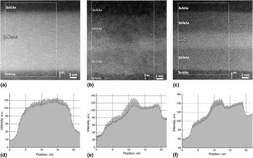
The electrophysical and structural properties of InAlAs/InGaAs/InAlAs quantum wells (QWs) with thin InAs inserts were investigated by means of Hall effect measurements and scanning transmission electron microscopy. The analyzed heterostructures are nearly the same ones using for high electron mobility transistors manufacturing except for heavily doped contact top layer. The increase of the electron mobility and concentration in the heterostructures with thin InAs layers in the center of the InGaAs QW as compared with the uniform QW was found and this effect strongly depended on the technological conditions during growth of the InAs inserts. The dependence of the InAs insert structural quality and heterointerface width on the As4 beam equivalent pressure PAs was revealed. The decreased PAs is required for obtaining uniform and smooth InAs inserts as opposed to higher PAs resulting in the interface spreading and lateral composition inhomogeneity of the InAs insert.

Type
Articles
Copyright
Copyright © Materials Research Society 2015 

Access options

Get access to the full version of this content by using one of the access options below. (Log in options will check for institutional or personal access. Content may require purchase if you do not have access.)

References

REFERENCES

Kim, D-H. and del Alamo, J.A.: 30-nm InAs PHEMTs with f T = 644 GHz and f max = 681 GHz. IEEE Electron Device Lett. 31, 806 (2010).Google Scholar
Drouot, V., Gendry, M., Santinelli, C., Letartre, X., Tardy, J., Viktorovitch, P., Hollinger, G., Ambri, M., and Pitaval, M.: Design and growth investigations of strained InxGa1–xAs/InAlAs/InP heterostructures for high electron mobility transistor application. IEEE Trans. Electron Devices 43, 1326 (1996).Google Scholar
Bollaert, S., Cordier, Y., Zaknoune, M., Happy, H., Hoel, V., Lepilliet, S., Théron, D., and Cappy, A.: The indium content in metamorphic InxAl1–xAs/InxGa1–xAs HEMTs on GaAs substrate: A new structure parameter. Solid-State Electron. 44, 1021 (2000).Google Scholar
Galiev, G.B., Vasil’evskii, I.S., Klimov, E.А., Pushkarev, S.S., Klochkov, A.N., Maltsev, P.P., Presniakov, M.Yu., Trunkin, I.N., and Vasiliev, A.L.: Effect of (1 0 0) GaAs substrate misorientation on electrophysical parameters, structural properties and surface morphology of metamorphic HEMT nanoheterostructures InGaAs/InAlAs. J. Cryst. Growth 392, 11 (2014).Google Scholar
Maeda, N., Ito, H., Enoki, T., and Ishii, Y.: Dependence on channel potential structures of I–V characteristics in InAlAs/InGaAs pseudomorphic high electron mobility transistors. J. Appl. Phys. 81, 1552 (1997).Google Scholar
Akazaki, T., Nitta, J., Takayanagi, H., Enoki, T., and Arai, K.: Highly confined two-dimensional electron gas in an In0.52AI0.48As/In0.52Ga0.47As modulation-doped structure with a strained InAs quantum well. J. Electron. Mater. 25, 745 (1996).Google Scholar
Nakayama, T. and Miyamoto, H.: Modulation doped structure with thick strained InAs channel beyond the critical thickness. J. Cryst. Growth 201202, 782 (1999).Google Scholar
Richter, A., Koch, M., Matsuyama, T., Heyn, Ch., and Merkt, U.: Transport properties of modulation-doped InAs-inserted-channel In0.75Al0.25As/In0.75Ga0.25As structures grown on GaAs substrates. Appl. Phys. Lett. 77, 3227 (2000).CrossRefGoogle Scholar
Kulbachinskii, V.A., Yuzeeva, N.A., Galiev, G.B., Klimov, E.A., Vasil’evskiі, I.S., Khabibullin, R.A., and Ponomarev, D.S.: Electron effective masses in an InGaAs quantum well with InAs and GaAs inserts. Semicond. Sci. Technol. 27, 035021 (2012).Google Scholar
Šilenas, A., Požela, Yu., Požela, K., Jucienė, V., Vasil’evskii, I.S., Galiev, G.B., Pushkarev, S.S., and Klimov, E.A.: Maximum drift velocity of electrons in selectively doped InAlAs/InGaAs/InAlAs heterostructures with InAs inserts. Semiconductors 47, 372 (2013).Google Scholar
Sexl, M., Böhm, G., Xu, D., Heiβ, H., Kraus, S., Tränkle, G., and Weiman, G.: MBE growth of double-sided doped InAlAs/InGaAs HEMTs with an InAs layer inserted in the channel. J. Cryst. Growth 175176, 915 (1997).Google Scholar
Požela, K., Šilėnas, A., Požela, J., Jucienė, V., Galiev, G.B., Vasil’evskii, I.S., and Klimov, E.A.: Effects of phonon confinement on high-electric field electron transport in an InGaAs/InAlAs quantum well with an inserted InAs barrier. Appl. Phys. A 109, 233 (2012).Google Scholar
Stangl, J., Holý, V., and Bauer, G.: Structural properties of self-organized semiconductor nanostructures. Rev. Mod. Phys. 76, 725 (2004).Google Scholar
Sakaki, H., Noda, T., Hirakawa, K., Tanaka, M., and Matsusue, T.: Interface roughness scattering in GaAs/AlAs quantum wells. Appl. Phys. Lett. 51, 1934 (1987).CrossRefGoogle Scholar
Tournie, E. and Ploog, K.H.: Surface stoichiometry, epitaxial morphology and strain relaxation during molecular beam epitaxy of highly strained InAs/Ga0.47In0.53As heterostructures. J. Cryst. Growth 135, 97 (1994).Google Scholar
Vurgaftman, I., Meyer, J.R., and Ram-Mohan, L.R.: Band parameters for III–V compound semiconductors and their alloys. J. App. Phys. 89, 5815 (2001).Google Scholar
Watanabe, A., Isu, T., Hata, M., and Katayama, Y.: Investigation of InP surface under arsenic pressure using RHEED-TRAXS. J. Cryst. Growth 115, 371 (1991).CrossRefGoogle Scholar