Hostname: page-component-78c5997874-fbnjt Total loading time: 0 Render date: 2024-11-02T23:42:17.436Z Has data issue: false hasContentIssue false

Transport properties of VSe2 monolayers separated by bilayers of BiSe

Published online by Cambridge University Press:  21 December 2015

Omar K. Hite*
Affiliation:
Department of Chemistry, University of Oregon, Eugene, OR 97403-1253, USA
Michael Nellist
Affiliation:
Department of Chemistry, University of Oregon, Eugene, OR 97403-1253, USA
Jeffery Ditto
Affiliation:
Department of Chemistry, University of Oregon, Eugene, OR 97403-1253, USA
Matthias Falmbigl
Affiliation:
Department of Chemistry, University of Oregon, Eugene, OR 97403-1253, USA
David C. Johnson*
Affiliation:
Department of Chemistry, University of Oregon, Eugene, OR 97403-1253, USA
*
a) Address all correspondence to this author. e-mail: [email protected]
Get access

Abstract

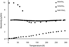
The [(BiSe)1+δ]1(VSe2)1 heterostructure was characterized structurally and electrically to determine the effects of interlayer interaction on the charge density wave (CDW) found in VSe2 and compared to previously reported [(SnSe)1.15]1(VSe2)1. Out-of-plane x-ray diffraction scans contain reflections that can be indexed as 00l reflections of a BiSe–VSe2 supercell. Structure refinement indicates that the VSe2 layer is very similar structurally to that found in [(SnSe)1.15]1(VSe2)1. Scanning transmission electron microscopy images show a turbostratically disordered layer structure and the formation of anti-phase boundaries in the BiSe bilayer. The [(BiSe)1+δ]1(VSe2)1 heterostructure is metallic with a negative Hall coefficient, in contrast to the positive Hall coefficient found for [(SnSe)1.15]1(VSe2)1. The CDW found [(SnSe)1.15]1(VSe2)1 is not present in [(BiSe)1+δ]1(VSe2)1. This work illustrates the importance of inter constituent interactions in determining the transport properties of single layer films.

Type
Invited Articles
Copyright
Copyright © Materials Research Society 2015 

Access options

Get access to the full version of this content by using one of the access options below. (Log in options will check for institutional or personal access. Content may require purchase if you do not have access.)

References

REFERENCES

Geim, A.K.: Graphene: Status and prospects. Science 324(5934), 1530 (2009).CrossRefGoogle Scholar
Wang, Q.H., Kalantar-Zadeh, K., Kis, A., Coleman, J.N., and Strano, M.S.: Electronics and optoelectronics of two-dimensional transition metal dichalcogenides. Nat. Nanotechnol. 7(11), 699712 (2012).CrossRefGoogle ScholarPubMed
Wang, H., Yuan, H., Hong, S.S., Li, Y., and Cui, Y.: Physical and chemical tuning of two-dimensional transition metal dichalcogenides. Chem. Soc. Rev. 44(9), 26642680 (2015).CrossRefGoogle ScholarPubMed
El-Bana, M.S., Wolverson, D., Russo, S., Balakrishnan, G., Paul, D.M., and Bending, S.J.: Superconductivity in two-dimensional NbSe2 field effect transistors. Supercond. Sci. Technol. 26(12), 125020 (2013).CrossRefGoogle Scholar
Anderson, M.D., Heideman, C.L., Lin, Q., Smeller, M., Kokenyesi, R., Herzing, A.A., Anderson, I.M., Keszler, D.A., Zschack, P., and Johnson, D.C.: Size-dependent structural distortions in one-dimensional nanostructures. Angew. Chem., Int. Ed. 52(7), 19821985 (2013).CrossRefGoogle ScholarPubMed
Geim, A.K. and Grigorieva, I.V.: Van der Waals heterostructures. Nature 499(7459), 419425 (2013).CrossRefGoogle ScholarPubMed
Zeng, Q., Wang, H., Fu, W., Gong, Y., Zhou, W., Ajayan, P.M., Lou, J., and Liu, Z.: Band engineering for novel two-dimensional atomic layers. Small 11(16), 18681884 (2015).CrossRefGoogle ScholarPubMed
Qian, X., Liu, J., Fu, L., and Li, J.: Quantum spin hall effect and topological field effect transistor in two-dimensional transition metal dichalcogenide. Science 346(6215), 13441347 (2014).Google Scholar
Yang, W., Chen, G., Shi, Z., Liu, C-C., Zhang, L., Xie, G., Cheng, M., Wang, D., Yang, R., Shi, D., Watanabe, K., Taniguchi, T., Yao, Y., Zhang, Y., and Zhang, G.: Epitaxial growth of single-domain graphene on hexagonal boron nitride. Nat. Mater. 12(9), 792797 (2013).CrossRefGoogle ScholarPubMed
Heideman, C.L., Tepfer, S., Lin, Q., Rostek, R., Zschack, P., Anderson, M.D., Anderson, I.M., and Johnson, D.C.: Designed synthesis, structure, and properties of a family of ferecrystalline compounds [(PbSe)1.00]m(MoSe2)n . J. Am. Chem. Soc. 135(30), 1105511062 (2013).Google Scholar
Bayard, M. and Sienko, M.J.: Anomalous electrical and magnetic properties of vanadium diselenide. J. Solid State Chem. 19(4), 325329 (1976).Google Scholar
Xu, K., Chen, P., Li, X., Wu, C., Guo, Y., Zhao, J., Wu, X., and Xie, Y.: Ultrathin nanosheets of vanadium diselenide: A metallic two-dimensional material with ferromagnetic charge-density-wave behavior. Angew. Chem. Int. Ed. 52(40), 1047710481 (2013).CrossRefGoogle ScholarPubMed
Yang, J., Wang, W., Liu, Y., Du, H., Ning, W., Zheng, G., Jin, C., Han, Y., Wang, N., Yang, Z., Tian, M., and Zhang, Y.: Thickness dependence of the charge-density-wave transition temperature in VSe2 . Appl. Phys. Lett. 105(6), 063109 (2014).Google Scholar
Atkins, R., Disch, S., Jones, Z., Haeusler, I., Grosse, C., Fischer, S.F., Neumann, W., Zschack, P., and Johnson, D.C.: Synthesis, structure and electrical properties of a new tin vanadium selenide. J. Solid State Chem. 202, 128133 (2013).Google Scholar
Falmbigl, M., Fiedler, A., Atkins, R.E., Fischer, S.F., and Johnson, D.C.: Suppressing a charge density wave by changing dimensionality in the ferecrystalline compounds ([SnSe]1.15)1(VSe2)n . Nano Lett. 15(2) 943948 (2015).Google Scholar
Zhou, W.Y., Meetsma, A., de Boer, J.L., and Wiegers, G.A.: Characterization and electrical transport properties of the misfit layer compounds (BiSe)1.10NbSe2 and (BiSe)1.09TaSe2 . Mater. Res. Bull. 27, 563572 (1992).Google Scholar
Wiegers, G.A.: Misfit layer compounds: Structures and physical properties. Prog. Solid State Chem. 24, 1139 (1996).Google Scholar
Petříček, V., Cisarova, I., de Boer, J.L., Zhou, W., Meetsma, A., Wiegers, G.A., and van Smaalen, S.: The modulated structure of the commensurate misfit-layer compound (BiSe)1.09TaSe2 . Acta Crystallogr., Sect. B: Struct. Sci. 49(2), 258266 (1993).Google Scholar
Fister, L.: Deposition system for the synthesis of modulated, ultrathin-film composites. J. Vac. Sci. Technol. A 11(6), 3014 (1993).CrossRefGoogle Scholar
Schaffer, M., Schaffer, B., and Ramasse, Q.: Sample preparation for atomic-resolution STEM at low voltages by FIB. Ultramicroscopy 114, 6271 (2012).Google Scholar
van der Pauw, L.J.: A method of measuring the resistivity and hall coefficient on lamellae of arbitrary shape. Philips Tech. Rev. 26, 220224 (1958).Google Scholar
Heideman, C., Nyugen, N., Hanni, J., Lin, Q., Duncombe, S., Johnson, D.C., and Zschack, P.: The synthesis and characterization of new [(BiSe)1.10]m[NbSe2]n, [(PbSe)1.10]m[NbSe2]n, [(CeSe)1.14]m[NbSe2]n and [(PbSe)1.12]m[TaSe2]n misfit layered compounds. J. Solid State Chem. 181(7), 17011706 (2008).CrossRefGoogle Scholar
Alemayehu, M.B., Falmbigl, M., Grosse, C., Ta, K., Fischer, S.F., and Johnson, D.C.: Structural and electrical properties of a new ([SnSe]1.16)m(NbSe2) polytype. J. Alloys Compd. 619, 816868 (2015).Google Scholar
Mitchson, G., Falmbigl, M., Ditto, J., and Johnson, D.C.: Antiphase boundaries in the turbostratically disordered misfit compound (BiSe)1+δNbSe2 . Inorg. Chem. (2015). doi: 10.1021/acs.inorgchem.5b01648, published online 14 October.Google Scholar
Grosse, C., Atkins, R., Kirmse, H., Mogilatenko, A., Neumann, W., and Johnson, D.C.: Local structure and defect chemistry of [(SnSe)1.15] m(TaSe2) ferecrystals—A new type of layered intergrowth compound. J. Alloys Compd. 579, 507515 (2013).Google Scholar