Hostname: page-component-cd9895bd7-jn8rn Total loading time: 0 Render date: 2024-12-24T03:41:31.588Z Has data issue: false hasContentIssue false

Solution-processed oxide thin film transistors on shape memory polymer enabled by photochemical self-patterning

Published online by Cambridge University Press:  14 September 2018

Trey B. Daunis*
Affiliation:
Department of Materials Science and Engineering, The University of Texas at Dallas, Richardson, Texas 75080, USA
Diego Barrera
Affiliation:
Department of Materials Science and Engineering, The University of Texas at Dallas, Richardson, Texas 75080, USA
Gerardo Gutierrez-Heredia
Affiliation:
Department of Materials Science and Engineering, The University of Texas at Dallas, Richardson, Texas 75080, USA; and Centro de Investigaciones en Optica, León 37150, Guanajuato, México
Ovidio Rodriguez-Lopez
Affiliation:
Department of Electrical and Computer Engineering, Department of Bioengineering, The University of Texas at Dallas, Richardson, Texas 75080, USA
Jian Wang
Affiliation:
Department of Materials Science and Engineering, The University of Texas at Dallas, Richardson, Texas 75080, USA
Walter E. Voit
Affiliation:
Department of Materials Science and Engineering, Department of Electrical and Computer Engineering, Department of Bioengineering, The University of Texas at Dallas, Richardson, Texas 75080, USA
Julia W.P. Hsu
Affiliation:
Department of Materials Science and Engineering, The University of Texas at Dallas, Richardson, Texas 75080, USA
*
a)Address all correspondence to this author. e-mail: [email protected]
Get access

Abstract

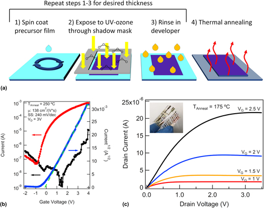
Solution-processed metal oxide electronics on flexible substrates can enable applications from military to health care. Due to limited thermal budgets and mismatched coefficients of thermal expansion between oxides and substrates, achieving good performance in solution-processed oxide films remains a challenge. Additionally, the use of traditional photolithographic processes is incompatible with low-cost, high-throughput roll-to-roll processing. Here, we demonstrate solution-deposited oxide thin film transistors (TFTs) on a shape memory polymer substrate, which offers unique control of final device shape and modulus. The key enabling step is the exposure of the precursor film to UV-ozone through a shadow mask to perform patterning and photochemical conversion simultaneously. These TFTs exhibit mobility up to 160 cm2/(V s), subthreshold swing as low as 110 mV/dec, and threshold voltage between −2 and 0 V, while maintaining compatibility with a flexible form factor at processing temperatures below 250 °C.

Type
Invited Paper
Copyright
Copyright © Materials Research Society 2018 

Access options

Get access to the full version of this content by using one of the access options below. (Log in options will check for institutional or personal access. Content may require purchase if you do not have access.)

References

REFERENCES

Khan, Y., Ostfeld, A.E., Lochner, C.M., Pierre, A., and Arias, A.C.: Monitoring of vital signs with flexible and wearable medical devices. Adv. Mater. 28, 4373 (2016).CrossRefGoogle ScholarPubMed
Choi, M.C., Kim, Y., and Ha, C.S.: Polymers for flexible displays: From material selection to device applications. Prog. Polym. Sci. 33, 581 (2008).CrossRefGoogle Scholar
Zhao, Q., Qi, H.J., and Xie, T.: Recent progress in shape memory polymer: New behavior, enabling materials, and mechanistic understanding. Prog. Polym. Sci. 49–50, 79 (2015).CrossRefGoogle Scholar
Ware, T., Simon, D., Hearon, K., Liu, C., Shah, S., Reeder, J., Khodaparast, N., Kilgard, M.P., Maitland, D.J., Rennaker, R.L., and Voit, W.E.: Three-dimensional flexible electronics enabled by shape memory polymer substrates for responsive neural interfaces. Macromol. Mater. Eng. 297, 1193 (2012).CrossRefGoogle ScholarPubMed
Reeder, J., Kaltenbrunner, M., Ware, T., Arreaga-Salas, D., Avendano-Bolivar, A., Yokota, T., Inoue, Y., Sekino, M., Voit, W., Sekitani, T., and Someya, T.: Mechanically adaptive organic transistors for implantable electronics. Adv. Mater. 26, 4967 (2014).CrossRefGoogle ScholarPubMed
Gutierrez-Heredia, G., Rodriguez-Lopez, O., Garcia-Sandoval, A., and Voit, W.E.: Highly stable indium–gallium–zinc–oxide thin-film transistors on deformable softening polymer substrates. Adv. Electron. Mater. 3, 1700221 (2017).CrossRefGoogle Scholar
MacDonald, W.A.: Engineered films for display technologies. J. Mater. Chem. 14, 4 (2004).CrossRefGoogle Scholar
Voit, W., Ware, T., Dasari, R.R., Smith, P., Danz, L., Simon, D., Barlow, S., Marder, S.R., and Gall, K.: High-strain shape-memory polymers. Adv. Funct. Mater. 20, 162 (2010).CrossRefGoogle Scholar
Fu, Q., Cao, C-B., and Zhu, H-S.: Preparation of alumina films from a new sol–gel route. Thin Solid Films 348, 99 (1999).CrossRefGoogle Scholar
Heo, S.J., Yoon, D.H., Jung, T.S., and Kim, H.J.: Recent advances in low-temperature solution-processed oxide backplanes. J. Inf. Disp. 14, 79 (2013).CrossRefGoogle Scholar
Brinker, C.J. and Scherer, G.W.: Sol–Gel Science: The Physics and Chemistry of Sol–Gel Processing (Academic Press, Cambridge, MA, 1990); p. 68.Google Scholar
Liu, A., Zhu, H., Guo, Z., Meng, Y., and Liu, G.: Solution combustion synthesis: Low-temperature processing for p-type Cu:NiO thin films for transparent electronics. Adv. Mater. 29, 1701599 (2017).CrossRefGoogle ScholarPubMed
Kim, M-G., Kanatzidis, M.G., Facchetti, A., and Marks, T.J.: Low-temperature fabrication of high-performance metal oxide thin-film electronics via combustion processing. Nat. Mater. 10, 382 (2011).CrossRefGoogle ScholarPubMed
Wang, B., Yu, X., Guo, P., Huang, W., Zeng, L., Zhou, N., Chi, L., Bedzyk, M.J., Chang, R.P.H., Marks, T.J., and Facchetti, A.: Solution-processed all-oxide transparent high-performance transistors fabricated by spray-combustion synthesis. Adv. Electron. Mater. 2, 1500427 (2016).CrossRefGoogle Scholar
Tetzner, K., Lin, Y.H., Regoutz, A., Seitkhan, A., Payne, D.J., and Anthopoulos, T.D.: Sub-second photonic processing of solution-deposited single layer and heterojunction metal oxide thin-film transistors using a high-power xenon flash lamp. J. Mater. Chem. C 5, 11724 (2017).CrossRefGoogle Scholar
Kim, Y-H., Heo, J-S., Kim, T-H., Park, S., Yoon, M-H., Kim, J., Oh, M.S., Yi, G-R., Noh, Y-Y., and Park, S.K.: Flexible metal-oxide devices made by room-temperature photochemical activation of sol–gel films. Nature 489, 128 (2012).CrossRefGoogle ScholarPubMed
Hwang, Y.H., Seo, S-J., Jeon, J-H., and Bae, B-S.: Ultraviolet photo-annealing process for low temperature processed sol–gel zinc tin oxide thin film transistors. Electrochem. Solid-State Lett. 15, H91 (2012).CrossRefGoogle Scholar
Dellis, S., Isakov, I., Kalfagiannis, N., and Tetzner, K.: Rapid laser-induced photochemical conversion of sol–gel precursors to In2O3 layers and their application in thin-film transistors. J. Mater. Chem. C 5, 3673 (2017).CrossRefGoogle Scholar
Jun, T., Song, K., Jeong, Y., Woo, K., Kim, D., Bae, C., and Moon, J.: High-performance low-temperature solution-processable ZnO thin film transistors by microwave-assisted annealing. J. Mater. Chem. 21, 1102 (2011).CrossRefGoogle Scholar
Park, S., Kim, K-H., Jo, J-W., Sung, S., Kim, K-T., Lee, W-J., Kim, J., Kim, H.J., Yi, G-R., Kim, Y-H., Yoon, M-H., and Park, S.K.: In-depth studies on rapid photochemical activation of various sol-gel metal oxide films for flexible transparent electronics. Adv. Funct. Mater. 25, 2807 (2015).CrossRefGoogle Scholar
Park, Y.M., Desai, A., Salleo, A., and Jimison, L.: Solution-processable zirconium oxide gate dielectrics for flexible organic field effect transistors operated at low voltages. Chem. Mater. 25, 2571 (2013).CrossRefGoogle Scholar
Ware, T., Simon, D., Arreaga-Salas, D.E., Reeder, J., Rennaker, R., Keefer, E.W., and Voit, W.: Fabrication of responsive, softening neural interfaces. Adv. Funct. Mater. 22, 3470 (2012).CrossRefGoogle Scholar
Daunis, T.B., Gutierrez-Heredia, G., Rodriguez-Lopez, O., Wang, J., Voit, W.E., and Hsu, J.W.P.: Solution-deposited Al2O3 dielectric towards fully-patterned thin film transistors on shape memory polymer. Proc. SPIE 10105, 101051Z (2017).Google Scholar
Lee, D.H., Chang, Y.J., and Herman, G.S.: A general route to printable high-mobility transparent amorphous oxide semiconductors. Adv. Mater. 19, 843 (2007).CrossRefGoogle Scholar
Rim, Y.S., Chen, H., Liu, Y., Bae, S-H., Kim, H.J., and Yang, Y.: Direct light pattern integration of low-temperature solution-processed all-oxide flexible electronics. ACS Appl. Mater. Interfaces 8, 9680 (2014).Google ScholarPubMed
Jo, J-W., Kim, J., Kim, K-T., Kang, J-G., Kim, M-G., Kim, K-H., Ko, H., Kim, Y-H., and Park, S.K.: Highly stable and imperceptible electronics utilizing photoactivated heterogeneous sol–gel metal-oxide dielectrics and semiconductors. Adv. Mater. 27, 1182 (2015).CrossRefGoogle ScholarPubMed
Honda, F. and Hirokawa, K.: X-ray photoelectron spectroscopic observation of nitrogen-containing gases adsorbed at high pressures on some transition metals. J. Electron Spectrosc. Relat. Phenom. 10, 125 (1977).CrossRefGoogle Scholar
Baltrusaitis, J., Jayaweera, P.M., and Grassian, V.H.: XPS study of nitrogen dioxide adsorption on metal oxide particle surfaces under different environmental conditions. Phys. Chem. Chem. Phys. 11, 8295 (2009).CrossRefGoogle ScholarPubMed
Hwang, J., Lee, K., Jeong, Y., Lee, Y.U., Pearson, C., Petty, M.C., and Kim, H.: UV-assisted low temperature oxide dielectric films for TFT applications. Adv. Mater. Interfaces 1, 1400206 (2014).CrossRefGoogle Scholar
Yu, X., Smith, J., Zhou, N., Zeng, L., Guo, P., Xia, Y., Alvarez, A., Aghion, S., Lin, H., Yu, J., Chang, R.P.H., Bedzyk, M.J., Ferragut, R., Marks, T.J., and Facchetti, A.: Spray-combustion synthesis: Efficient solution route to high-performance oxide transistors. Proc. Natl. Acad. Sci. U. S. A. 112, 3217 (2015).CrossRefGoogle ScholarPubMed
Sanctis, S., Hoffmann, R.C., Bruns, M., and Schneider, J.J.: Direct photopatterning of solution-processed amorphous indium zinc oxide and zinc tin oxide semiconductors—A chimie douce molecular precursor approach to thin film electronic oxides. Adv. Mater. Interfaces 5, 1800324 (2018).CrossRefGoogle Scholar
Nayak, P.K., Hedhili, M.N., Cha, D., and Alshareef, H.N.: High performance In2O3 thin film transistors using chemically derived aluminum oxide dielectric. Appl. Phys. Lett. 103, 033518 (2013).CrossRefGoogle Scholar
Xu, Y., Li, X., Zhu, L., and Zhang, J.: Defect modification in ZnInSnO transistor with solution-processed Al2O3 dielectric by annealing. Mater. Sci. Semicond. Process. 46, 23 (2016).CrossRefGoogle Scholar
Xu, W., Wang, H., Xie, F., Chen, J., Cao, H., and Xu, J-B.: Facile and environmentally friendly solution-processed aluminum oxide dielectric for low-temperature, high-performance oxide thin-film transistors. ACS Appl. Mater. Interfaces 7, 5803 (2015).CrossRefGoogle ScholarPubMed
Zhang, Y., Huang, G., Duan, L., Dong, G., Zhang, D., and Qiu, Y.: Full-solution-processed high mobility zinc-tin-oxide thin-film-transistors. Sci. China: Technol. Sci. 59, 1407 (2016).CrossRefGoogle Scholar
Liu, A., Zhu, H., Sun, H., Xu, Y., and Noh, Y-Y.: Solution processed metal oxide high-κ dielectrics for emerging transistors and circuits. Adv. Mater. 30, 1706364 (2018).CrossRefGoogle Scholar