Hostname: page-component-586b7cd67f-2plfb Total loading time: 0 Render date: 2024-11-24T17:51:49.231Z Has data issue: false hasContentIssue false

Optical properties of Si nanowires: Dependence on substrate crystallographic orientation and light polarization

Published online by Cambridge University Press:  13 March 2015

Juan A. Badán*
Affiliation:
Instituto de Física & CINQUIFIMA, Facultad de Ingeniería, Universidad de la República, CP 11000, Montevideo, Uruguay
Ricardo E. Marotti
Affiliation:
Instituto de Física & CINQUIFIMA, Facultad de Ingeniería, Universidad de la República, CP 11000, Montevideo, Uruguay
Enrique A. Dalchiele
Affiliation:
Instituto de Física & CINQUIFIMA, Facultad de Ingeniería, Universidad de la República, CP 11000, Montevideo, Uruguay
Daniel Ariosa
Affiliation:
Instituto de Física & CINQUIFIMA, Facultad de Ingeniería, Universidad de la República, CP 11000, Montevideo, Uruguay
Francisco Martín
Affiliation:
Lab. de Materiales y Superficies (Unidad Asociada al CSIC), Dptos. de Física Aplicada & Ingeniería Química, Universidad de Málaga, E29071 Málaga, Spain
Dietmar Leinen
Affiliation:
Lab. de Materiales y Superficies (Unidad Asociada al CSIC), Dptos. de Física Aplicada & Ingeniería Química, Universidad de Málaga, E29071 Málaga, Spain
Efrain Ochoa
Affiliation:
Lab. de Materiales y Superficies (Unidad Asociada al CSIC), Dptos. de Física Aplicada & Ingeniería Química, Universidad de Málaga, E29071 Málaga, Spain
José R. Ramos-Barrado
Affiliation:
Lab. de Materiales y Superficies (Unidad Asociada al CSIC), Dptos. de Física Aplicada & Ingeniería Química, Universidad de Málaga, E29071 Málaga, Spain
*
a)Address all correspondence to this author. e-mail: [email protected]
Get access

Abstract

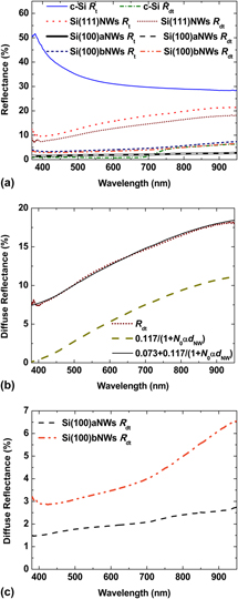
Optical properties of Si nanowire (SiNW) arrays prepared on p-doped Si(111) and Si(100) substrates were studied. SiNWs were synthesized by self-assembly electroless metal deposition nanoelectrochemistry in an ionic silver HF solution through selective etching. Total reflectance (Rt) and total diffuse reflectance (Rdt) of SiNWs change drastically in comparison to polished Si. To understand these changes, diffuse reflectance (Rd) with polarized incident light was studied. For samples prepared on Si(111), the wave length integrated Rd (wIRd) shows maxima at certain angles of incidence θ, regardless of the incident light polarization. For samples prepared on Si(100), wIRd increases with θ and depends on incident light polarization. Also, Rd spectra show structures due to interference effects. Therefore, SiNWs prepared on Si(100) can be considered as thin films whose refractive index depends on light polarization. Moreover, Rdt of SiNWs prepared on Si(111) can be modeled as an ensemble of diffuse reflectors.

Type
Articles
Copyright
Copyright © Materials Research Society 2015 

Access options

Get access to the full version of this content by using one of the access options below. (Log in options will check for institutional or personal access. Content may require purchase if you do not have access.)

References

REFERENCES

Peng, K., Wang, X., and Lee, S.T.: Silicon nanowire array photoelectrochemical solar cells. Appl. Phys. Lett. 92, 163103 (2008).Google Scholar
Convertino, A., Cuscuna, M., and Martelli, F.: Optical reflectivity from highly disordered Si nanowire films. Nanotechnology 21, 355701 (2010).Google Scholar
Xie, W.Q., Oh, J.I., and Shen, W.Z.: Realization of effective light trapping and omnidirectional antireflection in smooth surface silicon nanowire arrays. Nanotechnology 22, 065704 (2011).CrossRefGoogle ScholarPubMed
Street, R.A., Wong, W.S., and Paulson, C.: Analytic model for diffuse reflectivity of silicon nanowire mats. Nano Lett. 9, 3494 (2009).Google Scholar
Lin, X.X., Hua, X., Huang, Z.G., and Shen, W.Z.: Realization of high performance silicon nanowire based solar cells with large size. Nanotechnology 24, 235402 (2013).CrossRefGoogle ScholarPubMed
Jiang, Y., Qin, R., Li, M., Wang, G., Ma, H., and Chang, F.: Effect of alkali treatment on the spectral response of silicon-nanowire solar cells. Mater. Sci. Semicond. Process. 17, 81 (2014).Google Scholar
Spurgeon, J.M., Atwater, H.A., and Lewis, N.S.: A comparison between the behavior of nanorod array and planar Cd(Se, Te) photoelectrodes. J. Phys. Chem. C 112, 6186 (2008).Google Scholar
Kayes, B.M., Atwater, H.A., and Lewis, N.S.: Comparison of the device physics principles of planar and radial p-n junction nanorod solar cells. J. Appl. Phys. 97, 114302 (2005).Google Scholar
Tena-Zaera, R., Ryan, M.A., Katty, A., Hodes, G., Bastide, S., and Levy-Clemént, C.: Fabrication and characterization of ZnO nanowires/CdSe/CuSCNeta-solar cell. C. R. Chim. 9, 717 (2006).Google Scholar
Baxter, J.B. and Aydil, E.S.: Nanowire based dye sensitized solar cells. Appl. Phys. Lett. 86, 053114 (2005).CrossRefGoogle Scholar
Wagner, R.S. and Ellis, W.C.: Vapor liquid solid mechanism of single crystal growth. Appl. Phys. Lett. 4, 89 (1964).Google Scholar
Morales, A.M. and Lieber, C.M.: A laser ablation method for synthesis of crystalline semiconductor nanowires. Science 279, 208 (1998).CrossRefGoogle ScholarPubMed
Zhang, Y.F., Tang, Y.H., Wang, N., Yu, D.P., Lee, C.S., Bello, I., and Lee, S.T.: Silicon nanowires prepared by laser ablation at high temperature. Appl. Phys. Lett. 72, 1835 (1998).Google Scholar
Schubert, L., Werner, P., Zakharov, N.D., Gerth, G., Kolb, F.M., Long, L., Gösele, U., and Tan, T.Y.: Silicon nanowhiskers grown on 〈111〉 Si substrates by molecular-beam epitaxy. Appl. Phys. Lett. 84, 4968 (2004).CrossRefGoogle Scholar
Juhasz, R., Kylmänen, K., Galeckas, A., and Linnros, J.: Size-reduced silicon nanowires: Fabrication and electrical characterization. Mater. Sci. Eng., C 25, 733 (2005).CrossRefGoogle Scholar
Stelzner, Th., Pietsch, M., Andrä, G., Falk, F., Ose, E., and Christiansen, S.: Silicon nanowire-based solar cells. Nanotechnology 19, 295203 (2008).Google Scholar
Lu, M., Li, M.K., Kong, L.B., Guo, X.Y., and Li, H.L.: Silicon quantum-wires arrays synthesized by chemical vapor deposition and its micro-structural properties. Chem. Phys. Lett. 374, 542 (2003).CrossRefGoogle Scholar
Peng, K-Q., Yan, Y-J., Gao, S-P., and Zhu, J.: Synthesis of large area silicon nanowire arrays via self assembly nanoelectrochemistry. Adv. Mater. 14, 1164 (2002).Google Scholar
Qiu, T., Wu, X.L., Mei, Y.F., Wan, G.J., Chu, P.K., and Siu, G.G.: From Si nanotubes to nanowires: Synthesis, characterization, and self-assembly. J. Cryst. Growth 227, 143 (2005).Google Scholar
Dalchiele, E.A., Martín, F., Leinen, D., Marotti, R.E., and Ramos-Barrado, J.R.: Synthesis, structure and photoelectrochemical properties of single crystalline silicon nanowire arrays. Thin Solid Films 518, 1804 (2010).CrossRefGoogle Scholar
Dalchiele, E.A., Martín, F., Leinen, D., Marotti, R.E., and Ramos-Barrado, J.R.: Single-crystalline silicon nanowire array-based photoelectrochemical cells. J. Electrochem. Soc. 156, K77 (2009).CrossRefGoogle Scholar
Wu, S-L., Zhang, T., Zheng, R-T., and Cheng, G-A.: Facile morphological control of single-crystalline silicon nanowires. Appl. Surf. Sci. 258, 9792 (2012).Google Scholar
Branz, H.M., Yost, V.E., Ward, S., Jones, K.M., To, B., and Stradins, P.: Nanostructured black silicon and the optical reflectance of graded-density surfaces. Appl. Phys. Lett. 94, 231121 (2009).CrossRefGoogle Scholar
Oh, J., Yuan, H-C., and Branz, H.M.: An 18.2%-efficient black-silicon solar cell achieved through control of carrier recombination in nanostructures. Nat. Nanotechnol. 7, 743 (2012).CrossRefGoogle ScholarPubMed
Sturmberg, B.C.P., Dossou, K.B., Botten, L.C., Asatryan, A.A., Paulton, C.G., de Sterke, C.M., and McPhedran, R.C.: Modal analysis of enhanced absorption in silicon nanowire arrays. Opt. Express 19, A1067 (2011).CrossRefGoogle ScholarPubMed
Bao, H. and Ruan, X.: Optical absorption enhancement in disordered vertical silicon nanowire arrays for photovoltaic applications. Opt. Lett. 35, 3378 (2010).Google Scholar
Lagos, N., Sigalas, M.M., and Niarchos, D.: The optical absorption of nanowire arrays. Phot. Nano. Fund. Appl. 9, 163 (2011).CrossRefGoogle Scholar
Yamaguchi, T., Shimizu, T., Morosawa, Y., Takase, K., Chen, T., Lu, S., Chien, H., and Shingubara, S.. Morphology dependence of optical reflectance properties for a high density array of silicon nanowires. Jpn. J. Appl. Phys. 53, 06JF10 (2014).CrossRefGoogle Scholar
Li, H., Wang, W., Zhao, L., Zhou, C., and Diao, H.: A new attempt at alkaline texturization of monocrystaline silicon with anionic surfactant as the additive. Jpn. J. Appl. Phys. 51, 10NA18 (2012).Google Scholar
Sun, L. and Tang, J.: A new texturing of monocrystalline silicon surface with sodium hypochlorite. Appl. Surf. Sci. 255, 9301 (2009).CrossRefGoogle Scholar
Nelkomsky, M. and Braunstein, R.: Interband transitions and exciton effects in semiconductors. Phys. Rev. B 5, 497 (1972).Google Scholar
Forman, R.A., Thurber, W.R., and Aspnes, D.E.: Second indirect band gap in silicon. Solid State Commun. 14, 1007 (1974).Google Scholar
Green, M.A. and Keevers, M.: Optical properties of intrinsic silicon at 300 K. Prog. Photovoltaics Res. Appl. 3, 189 (2007).Google Scholar
Silverman, M.P.: Waves and Grains (Princeton University Press, Princeton, NJ, 1998).Google Scholar
Oton, C.J., Gaburro, Z., Ghulinyan, M., Pancheri, L., Bettotti, P., Dal Negro, L., and Pavesi, L.: Scattering rings in optically anisotropic porous silicon. Appl. Phys. Lett. 81, 4919 (2002).Google Scholar
Gómez Rivas, J., Muskens, O.L., Borgström, M.T., Diedenhofen, S.L., and Bakkers, E.P.A.M.: Optical anisotropy of semiconductor nanowires. In One-Dimensional Nanostructures, Lecture Notes in Nanoscale Science and Technology, Vol. 3, Wang, Z.M. ed. (Springer, New York, NY, 2008); p. 137.Google Scholar