Hostname: page-component-586b7cd67f-dlnhk Total loading time: 0 Render date: 2024-11-28T03:15:54.057Z Has data issue: false hasContentIssue false

Diffusion process in BaSi2 film formation by thermal evaporation and its relation to electrical properties

Published online by Cambridge University Press:  22 June 2018

Kosuke O. Hara*
Affiliation:
Center for Crystal Science and Technology, University of Yamanashi, Kofu, Yamanashi 400-8511, Japan
Keisuke Arimoto
Affiliation:
Center for Crystal Science and Technology, University of Yamanashi, Kofu, Yamanashi 400-8511, Japan
Junji Yamanaka
Affiliation:
Center for Instrumental Analysis, University of Yamanashi, Kofu, Yamanashi 400-8510, Japan
Kiyokazu Nakagawa
Affiliation:
Center for Crystal Science and Technology, University of Yamanashi, Kofu, Yamanashi 400-8511, Japan
*
a)Address all correspondence to this author. e-mail: [email protected]
Get access

Abstract

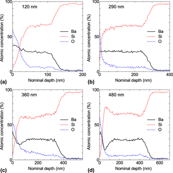
For fabricating photovoltaic BaSi2 films with controlled carrier density and suppressed oxidation by thermal evaporation, the mechanism determining the film composition from incongruently evaporated BaSi2 must be elucidated. We investigated the effects of source premelting, substrate temperature, and thickness on the structural and electrical properties of evaporated BaSi2 films. It is found by room-temperature deposition that the vapor composition continuously changes from being Ba-rich to being Si-rich. Source premelting suppresses the deposition of Ba-rich vapor. Deposition at 600–700 °C shows that BaSi2 forms through the mutual diffusion of Ba and Si, followed by surface oxidation by residual gas. Surface oxidation can be suppressed by a-axis-oriented growth. By changing the film thickness, the optimum thickness to obtain homogeneous films with suppressed oxidation is revealed. Sufficient diffusion leads to high film resistivities and low electron densities, which demonstrates a close relationship between the film composition and the electrical properties.

Type
Invited Feature Paper
Copyright
Copyright © Materials Research Society 2018 

Access options

Get access to the full version of this content by using one of the access options below. (Log in options will check for institutional or personal access. Content may require purchase if you do not have access.)

Footnotes

This paper has been selected as an Invited Feature Paper.

References

REFERENCES

Suemasu, T. and Usami, N.: Exploring the potential of semiconducting BaSi2 for thin-film solar cell applications. J. Phys. D: Appl. Phys. 50, 023001 (2016).CrossRefGoogle Scholar
Toh, K., Saito, T., and Suemasu, T.: Optical absorption properties of BaSi2 epitaxial films grown on a transparent silicon-on-insulator substrate using molecular beam epitaxy. Jpn. J. Appl. Phys. 50, 068001 (2011).CrossRefGoogle Scholar
Latiff, N.A.A., Yoneyama, T., Shibutami, T., Matsumaru, K., Toko, K., and Suemasu, T.: Fabrication and characterization of polycrystalline BaSi2 by RF sputtering. Phys. Status Solidi C 10, 17591761 (2013).CrossRefGoogle Scholar
Kumar, M., Umezawa, N., and Imai, M.: BaSi2 as a promising low-cost, earth-abundant material with large optical activity for thin-film solar cells: A hybrid density functional study. Appl. Phys. Express 7, 071203 (2014).CrossRefGoogle Scholar
Trinh, C.T., Nakagawa, Y., Hara, K.O., Takabe, R., Suemasu, T., and Usami, N.: Photoresponse properties of BaSi2 film grown on Si(100) by vacuum evaporation. Mater. Res. Express 3, 076204 (2016).CrossRefGoogle Scholar
Hara, K.O., Usami, N., Nakamura, K., Takabe, R., Baba, M., Toko, K., and Suemasu, T.: Determination of bulk minority-carrier lifetime in BaSi2 earth-abundant absorber films by utilizing a drastic enhancement of carrier lifetime by post-growth annealing. Appl. Phys. Express 6, 112302 (2013).CrossRefGoogle Scholar
Takabe, R., Hara, K.O., Baba, M., Du, W., Shimada, N., Toko, K., Usami, N., and Suemasu, T.: Influence of grain size and surface condition on minority-carrier lifetime in undoped n-BaSi2 on Si(111). J. Appl. Phys. 115, 193510 (2014).CrossRefGoogle Scholar
Suhara, T., Murata, K., Navabi, A., Hara, K.O., Nakagawa, Y., Trinh, C.T., Kurokawa, Y., Suemasu, T., Wang, K.L., and Usami, N.: Postannealing effects on undoped BaSi2 evaporated films grown on Si substrates. Jpn. J. Appl. Phys. 56, 05DB05 (2017).CrossRefGoogle Scholar
Shaalan, N.M., Hara, K.O., Trinh, C.T., Nakagawa, Y., and Usami, N.: Simple method for significant improvement of minority-carrier lifetime of evaporated BaSi2 thin film by sputtered-AlOx passivation. Mater. Sci. Semicond. Process. 76, 3741 (2018).CrossRefGoogle Scholar
Baba, M., Toh, K., Toko, K., Saito, N., Yoshizawa, N., Jiptner, K., Sekiguchi, T., Hara, K.O., Usami, N., and Suemasu, T.: Investigation of grain boundaries in BaSi2 epitaxial films on Si(111) substrates using transmission electron microscopy and electron-beam-induced current technique. J. Cryst. Growth 348, 7579 (2012).CrossRefGoogle Scholar
Suemasu, T.: Exploring the possibility of semiconducting BaSi2 for thin-film solar cell applications. Jpn. J. Appl. Phys. 54, 07JA01 (2015).CrossRefGoogle Scholar
Kumar, M., Umezawa, N., Zhou, W., and Imai, M.: Barium disilicide as a promising thin film photovoltaic absorber: Structural, electronic, and defect properties. J. Mater. Chem. A 5, 2529325302 (2017).CrossRefGoogle Scholar
Takabe, R., Deng, T., Kodama, K., Yamashita, Y., Sato, T., Toko, K., and Suemasu, T.: Impact of Ba to Si deposition rate ratios during molecular beam epitaxy on carrier concentration and spectral response of BaSi2 epitaxial films. J. Appl. Phys. 123, 045703 (2018).CrossRefGoogle Scholar
Kobayashi, M., Matsumoto, Y., Ichikawa, Y., Tsukada, D., and Suemasu, T.: Control of electron and hole concentrations in semiconducting silicide BaSi2 with impurities grown by molecular beam epitaxy. Appl. Phys. Express 1, 051403 (2008).CrossRefGoogle Scholar
Khan, M.A., Saito, T., Nakamura, K., Baba, M., Du, W., Toh, K., Toko, K., and Suemasu, T.: Electrical characterization and conduction mechanism of impurity-doped BaSi2 films grown on Si(111) by molecular beam epitaxy. Thin Solid Films 522, 9599 (2012).CrossRefGoogle Scholar
Khan, M.A., Hara, K.O., Nakamura, K., Du, W., Baba, M., Toh, K., Suzuno, M., Toko, K., Usami, N., and Suemasu, T.: Molecular beam epitaxy of boron doped p-type BaSi2 epitaxial films on Si(111) substrates for thin-film solar cells. J. Cryst. Growth 378, 201204 (2013).CrossRefGoogle Scholar
Khan, M.A., Hara, K.O., Du, W., Baba, M., Nakamura, K., Suzuno, M., Toko, K., Usami, N., and Suemasu, T.: In situ heavily p-type doping of over 1020 cm−3 in semiconducting BaSi2 thin films for solar cells applications. Appl. Phys. Lett. 102, 112107 (2013).CrossRefGoogle Scholar
Takabe, R., Baba, M., Nakamura, K., Du, W., Khan, M.A., Koike, S., Toko, K., Hara, K.O., Usami, N., and Suemasu, T.: Fabrication and characterizations of phosphorus-doped n-type BaSi2 epitaxial films grown by molecular beam epitaxy. Phys. Status Solidi C 10, 17531755 (2013).CrossRefGoogle Scholar
Hara, K.O., Hoshi, Y., Usami, N., Shiraki, Y., Nakamura, K., Toko, K., and Suemasu, T.: N-type doping of BaSi2 epitaxial films by phosphorus ion implantation and thermal annealing. Thin Solid Films 557, 9093 (2014).CrossRefGoogle Scholar
Hara, K.O., Usami, N., Baba, M., Toko, K., and Suemasu, T.: N-type doping of BaSi2 epitaxial films by arsenic ion implantation through a dose-dependent carrier generation mechanism. Thin Solid Films 567, 105108 (2014).CrossRefGoogle Scholar
Ajmal Khan, M. and Suemasu, T.: Donor and acceptor levels in impurity-doped semiconducting BaSi2 thin films for solar-cell application. Phys. Status Solidi A 214, 1700019 (2017).CrossRefGoogle Scholar
Hara, K.O., Trinh, C.T., Arimoto, K., Yamanaka, J., Nakagawa, K., Kurokawa, Y., Suemasu, T., and Usami, N.: Effects of deposition rate on the structure and electron density of evaporated BaSi2 films. J. Appl. Phys. 120, 045103 (2016).CrossRefGoogle Scholar
Tsukahara, D., Yachi, S., Takeuchi, H., Takabe, R., Du, W., Baba, M., Li, Y., Toko, K., Usami, N., and Suemasu, T.: p-BaSi2/n-Si heterojunction solar cells with conversion efficiency reaching 9.0%. Appl. Phys. Lett. 108, 152101 (2016).CrossRefGoogle Scholar
Yachi, S., Takabe, R., Takeuchi, H., Toko, K., and Suemasu, T.: Effect of amorphous Si capping layer on the hole transport properties of BaSi2 and improved conversion efficiency approaching 10% in p-BaSi2/n-Si solar cells. Appl. Phys. Lett. 109, 072103 (2016).CrossRefGoogle Scholar
Nakagawa, Y., Hara, K.O., Suemasu, T., and Usami, N.: Fabrication of single-phase polycrystalline BaSi2 thin films on silicon substrates by vacuum evaporation for solar cell applications. Jpn. J. Appl. Phys. 54, 08KC03 (2015).CrossRefGoogle Scholar
Takabe, R., Du, W., Ito, K., Takeuchi, H., Toko, K., Ueda, S., Kimura, A., and Suemasu, T.: Measurement of valence-band offset at native oxide/BaSi2 interfaces by hard X-ray photoelectron spectroscopy. J. Appl. Phys. 119, 025306 (2016).CrossRefGoogle Scholar
Hara, K.O., Yamamoto, C., Yamanaka, J., Arimoto, K., Nakagawa, K., and Usami, N.: Investigation on the origin of preferred a-axis orientation of BaSi2 films deposited on Si(100) by thermal evaporation. Mater. Sci. Semicond. Process. 72, 9398 (2017).CrossRefGoogle Scholar
Hara, K.O., Trinh, C.T., Kurokawa, Y., Arimoto, K., Yamanaka, J., Nakagawa, K., and Usami, N.: Post-annealing effects on the surface structure and carrier lifetime of evaporated BaSi2 films. Jpn. J. Appl. Phys. 56, 04CS07 (2017).CrossRefGoogle Scholar
Hara, K.O., Yamamoto, C., Yamanaka, J., Arimoto, K., Nakagawa, K., and Usami, N.: BaSi2 formation mechanism in thermally evaporated films and its application to reducing oxygen impurity concentration. Jpn. J. Appl. Phys. 57, 04FS01 (2018).CrossRefGoogle Scholar
Hara, K.O., Arimoto, K., Yamanaka, J., Nakagawa, K., and Usami, N.: Suppression of near-interface oxidation in thermally-evaporated BaSi2 films and its effects on preferred orientation and the rectification behavior of n-BaSi2/p+-Si diodes. MRS Adv. 3, 13871392 (2018).CrossRefGoogle Scholar
Balducci, G., Brutti, S., Ciccioli, A., Trionfetti, G., Palenzona, A., and Pani, M.: Thermodynamic properties of barium silicides from vapor pressure measurements and density functional calculations. Intermetallics 16, 10061012 (2008).CrossRefGoogle Scholar
Hara, K.O., Nakagawa, Y., Suemasu, T., and Usami, N.: Realization of single-phase BaSi2 films by vacuum evaporation with suitable optical properties and carrier lifetime for solar cell applications. Jpn. J. Appl. Phys. 54, 07JE02 (2015).CrossRefGoogle Scholar
Pani, M. and Palenzona, A.: The phase diagram of the Ba–Si system. J. Alloys Compd. 454, L1L2 (2008).CrossRefGoogle Scholar
Somer, M.: Vibrational spectra of the cluster anions [E4]4− in the metallic sodium and barium compounds Na4E4 and Ba2E4 (E = Si, Ge). Z. Anorg. Allg. Chem. 626, 24782480 (2000).3.0.CO;2-A>CrossRefGoogle Scholar
Terai, Y., Yamaguchi, H., Tsukamoto, H., Murakoso, N., Iinuma, M., and Suemasu, T.: Polarized Raman spectra of BaSi2 epitaxial film grown by molecular beam epitaxy. Jpn. J. Appl. Phys. 56, 05DD02 (2017).CrossRefGoogle Scholar
Hara, K.O., Trinh, C.T., Nakagawa, Y., Kurokawa, Y., Arimoto, K., Yamanaka, J., Nakagawa, K., and Usami, N.: Preferred orientation of BaSi2 thin films fabricated by thermal evaporation. JJAP Conf. Proc. 5, 011202 (2017).Google Scholar
Chandra, A., Wood, C.E.C., Woodard, D.W., and Eastman, L.F.: Surface and interface depletion corrections to free carrier-density determinations by Hall measurements. Solid-State Electron. 22, 645650 (1979).CrossRefGoogle Scholar
Liu, Y., Sun, Y., and Rockett, A.: A new simulation software of solar cells—wxAMPS. Sol. Energy Mater. Sol. Cells 98, 124128 (2012).CrossRefGoogle Scholar
Du, W., Baba, M., Toko, K., Hara, K.O., Watanabe, K., Sekiguchi, T., Usami, N., and Suemasu, T.: Analysis of the electrical properties of Cr/n-BaSi2 Schottky junction and n-BaSi2/p-Si heterojunction diodes for solar cell applications. J. Appl. Phys. 115, 223701 (2014).CrossRefGoogle Scholar
Morita, K., Inomata, Y., and Suemasu, T.: Optical and electrical properties of semiconducting BaSi2 thin films on Si substrates grown by molecular beam epitaxy. Thin Solid Films 508, 363366 (2006).CrossRefGoogle Scholar