1. Introduction
There is a strong interest in developing wide bandgap semiconductor heterojunction bipolar transistor (HBTs) for applications in wide bandwidth (initially 1-5GHz, eventually 5-25GHz) amplifiers employed in radar and communication systems. The GaN/AlGaN heterostructure system is an attractive one for these devices, Reference Shur[1] Reference Shur, Khan, Willander and Hartnagel[2] Reference Yoder[3] Reference Chow, Ramungul and Ghezzo[4] based on the remarkable success of the existing laser and light-emitting diode technology. Reference Nakamura, Senoh, Nagahama, Iwasa, Yamada, Matsushita, Kiyoku, Sugimoto, Kozaki, Umemoto, Sano and Chocho[5] The wide bandgaps of the nitrides allow for higher temperature device operation (e.g. an ni of 1015cm−3 would be reached at 300°C in Si, 500°C in GaAs, but in excess of 1000°C in GaN), reducing the thermal management issues. Pankove et.al. Reference Pankove, Leksono, Chang, Walker and Van Zeghbroeck[6] reported a GaN/SiC HBT operable to 535°C with gain of 100 and current density 1.84x10³A·cm−2. The barrier to hole injection from the p-SiC base to the GaN was measured to be 0.43eV, in good agreement with the band-offsets.
In this paper we report the fabrication and high temperature operation of a GaN/AlGaN HBT grown by a hybrid method. The active regions are grown by Molecular Beam Epitaxy (MBE) on a thick GaN buffer grown by Metal Organic Chemical Vapor Deposition (MOCVD). The device shows improved gain above 250°C as the hole density in the base increases and leads to lower base resistance. The device performance is still limited by the base doping, but there are various approaches that appear promising for improving this aspect.
2. Experimental
A highly resistive undoped buffer of ~2μm thick GaN, grown on c-plane (0001) sapphire, was used as the substrate for subsequent growth of the active device by RF-MBE. This structure formed a template for subsequent growth of the active regions by rf atomic nitrogen MBE at a rate of ~0.5μm·hr−1. Reference Van Hove, Chow, Klaassen, Hickman, Wowchak, Croswell and Polley[7] The Si-doped (~1018cm−3) GaN sub-collector (0.8μm thick) was followed by a 0.5μm, Si-doped (1017cm−3) GaN collector. Then a 0.15μm Mg-doped GaN base was deposited under process conditions calibrated for 1x1018cm−3 p-type carrier concentration as determined by Hall effect measurement. The epitaxy was completed with a 0.1μm thick, Si-doped (5x1017cm−3) Al0.15Ga0.85N emitter, a 0.05μm graded AlxGa1−xN (x = 0.15−0, 8x1018cm−3) region to a 0.2μm thick, Si-doped (8x1018cm−3) GaN contact layer.
Large area (~90μm diameter) devices were fabricated using a Cl2/Ar Inductively Coupled Plasma (ICP) etch process to expose both the base and sub-collector regions. Reference Shul, McClellan, Casalnuovo, Rieger, Pearton, Constantine, Barratt, Karlicek, Tran and Schurman[8] AZ5209E photoresist was used as an etch mask, and etching was performed in a Plasma Therm 790 system. The operating pressure was 2mTorr, and the source and rf chuck power were kept relatively lightly doped (300W and 40W, respectively) to minimize ion damage to the GaN. It is generally found that dry etch processes tend to produce N2-deficient surfaces on GaN that are strongly n-type. Reference Pearton, Shul, Penkove and Moustakas[9] This is an advantage when stopping at an existing n-type layer, because ohmic contact resistance will be improved. However to avoid this problem at the emitter-base junction, we terminated the etching ~100Å above the junction, then oxidized the surface using ozone, and stripped this in an acid solution. Ti/Al/Pt/Au n-type metallization and Ni/Pt/Au p-type metallization were deposited by e-beam evaporation to contact the emitter, base and sub-collector. A schematic of the completed structure is shown in Figure 1. Device characterization was performed with a HP 4145 parameter analyzer.

Figure 1. Schematic of GaN/AlGaN HBT
3. Results and Discussion
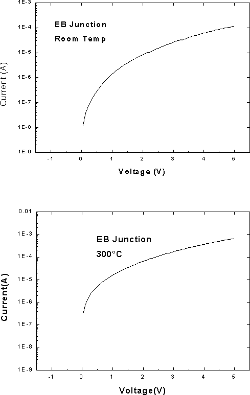
Figure 2 shows the forward current voltage (I-V) characteristics of the emitter-base junction at both 25 and 300°C. The relatively low hole concentration in the base at room temperature (a few 1017cm−3 based on the Mg ionization level of ~0.17eV), leads to a strong influence of the series resistance on the I-V characteristic. The low bias current at 300°C is about an order of magnitude higher than at 25°C due to the increase of thermionic current. The improvement in base contact I-V characteristic with increasing temperature is shown in Figure 3. As is fairly typical of p-contacts on GaN, the behavior is really that of a leaky Schottky-barrier at room temperature. Reference Lester, King, Zhang, Ramer, Hersee and Zolper[10] Reference King, Zhang, Ramer, Hersee and Lester[11] The best characteristics were obtained after annealing the Ni/Au at 700°C for 20secs, consistent with past reports. At higher annealing temperatures the I-V characteristics degraded and in some cases shorting of the devices was observed. We ascribe these observations to punch-through of the base metallization.

Figure 2. HBT emitter-base junction forward I-V characteristics at 25°C (top) and 300°C (bottom).

Figure 3. Ni/Pt/Au base contact I-V characteristics at 25°C (top) and 300°C (bottom).
The base-collector junction forward I-V characteristics are shown in Figure 4. Similar comments apply as for the e-b junction, with the high base resistance having a strong influence. For this reason it was not possible to obtain a meaningful ideality factor.

Figure 4. HBT base-collector junction forward I-V characteristics at 25°C (top) and 300°C (bottom).
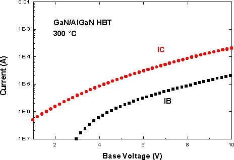
A Gummel plot for the HBT at 300°C is shown in Figure 5. The dc current gain is around 10 at this temperature because of the improvement in base resistance.

Figure 5. Gummel plot for a 90μm diameter GaN/AlGaN HBT at 300°C.
There are several approaches possible for improving the HBT performance. One would be to induce a higher hole concentration in the base through piezoelectric stress. A number of recent studies have demonstrated and analyzed the influence of the piezoelectric effort on III-nitride devices, Reference Bykhovski, Gelmont and Shur[12] Reference Yu, Asbeck, Lau and Sullivan[13] Reference Gaska, Yang, Bykhovski, Shur, Kaminskii and Soloviov[14] Reference Asbeck, Yu, Lau, Sullivan, Van Hove and Redwing[15] Reference Yu, Sullivan, Asbeck, Wang, Qiao and Lau[16] particularly heterostructure field effect transistors. In these structures piezo-induced electrons increase the conductivity in the channel of an AlGaN/GaN epitaxial structure. To induce more holes in the base of an HBT, one could consider placing as appropriate stress layer between the base and collector. A second alternative is to decrease base resistance by employing a lower gap material such as InGaN or SiC. There are still problems with these choices because of the difficulty in achieving high p-type doping in both materials- in InxGa1−xN there is a strong tendency for high n-type backgrounds, but p-type conductivity has been achieved for In compositions up to ~x=0.15, while the Al Acceptor in SiC has a large ionization level (~0.2eV).
The third alternative and probably the most attractive, is selective regrowth of the extrinsic base region. Reference Pearton, Abernathy and Ren[17] Reference Simawaki[18] The base doping typically represents a trade-off between base contact resistance and gain. By employing a separate regrowth step, it is possible to optimize both parameters. The intrinsic base material under the emitter can be relatively low in order to increase the minority carrier lifetime and hence the gain and base thickness reduced to decrease base transit time and hence speed. By selectively regrowing a heavily doped extrinsic base contact layer, the parasitic losses associated with the base contact resistance can be significantly reduced. Potential candidates for the regrown p+ material include GaAs (C) and GaP (C) which can attain hole concentrations in excess of 1021cm−3. Reference Pearton, Abernathy and Ren[17] The main issue would then be hole transport across the heterointerface, and compositional grading of the base material might also be necessary.
4. Summary and Conclusions
A GaN/AlGaN HBT operating at 300°C has been demonstrated, using an MBE-grown structure. Mesa formation has achieved with ICP Cl2/Ar dry etching, combined with a wet etch clean-up step at the emitter-base junction. Base resistance limits the performance in this initial device design, but several options exist for future development in this area.
Acknowledgments
The work at UF is partially supported by ONR grant N00014-98-1-0204 (J.C. Zolper) and a DARPA/EPRI grant MDA-972-98-1-0006 (E.R. Brown/J. Melcher). Sandia is a multiprogram laboratory operated by Sandia Corporation, a Lockheed-Martin company, for the US Department of Energy under contract DEAC04-95-AC85000.


