Introduction
Single crystal AlN is attractive for the fabrication of substrates for III-nitride epitaxial growth. Applications of wide-bandgap and high-temperature semiconductors include the development of blue/UV solid-state charge injection lasers, UV optical sources and detectors, high power microwave devices, high power switches, and high temperature applications. Enhanced III-nitride epitaxy on AlN substrates, due to smaller lattice mismatch, smaller thermal expansion mismatch and good chemical compatibility, may allow substantial improvement in the ability to manufacture these devices. In addition, very low defect material is needed for developing solid-state low noise and power devices for use in power supplies, communications, fire control, surveillance, and multifunctional RF systems using the nitride, wide-bandgap semiconductors. Foreign substrate induced defects have also been implicated in the performance of high power microwave devices. Substrates of AlN are also attractive for surface acoustic wave (SAW) applications, which would take advantage of the very high sound velocity in AlN. This would have application in high power, high frequency amplifiers for wireless communication base stations. The high thermal conductivity and electrically insulating properties of AlN are also attractive for high performance substrates where heat sinking is a key issue.
For III-nitride epitaxial growth, the preparation of nearly-atomically flat surface is required. Due to the extreme hardness of AlN, we have found that epitaxial-growth quality surfaces can be only achieved by using chemical-mechanical polishing (CMP) methods. The determination of the etching properties of single crystal substrates is of great importance for epitaxial growth and device preparation. We have studied the effects of KOH solution on the both the N and Al-terminated surfaces along the c-axis crystallographic direction on high-quality single crystal substrates. Also, we discuss a TEM-based method to unambiguously identify the N and Al-terminated faces along the c-axis.
Crystal Growth of Bulk Aln
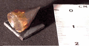
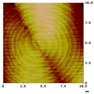
Several (see Fig. 1) AlN boules of up to 10mm of diameter have been produced at Crystal IS facilities using a sublimation-recondensation technique first developed for this material by Slack and McNelly [Reference Slack and McNelly1], which demonstrated crystal growth rates up to 0.3mm/hr. AFM imaging of the as-grown facets reveals interesting information about the growth mechanism of AlN. The atomic arrangement of the facets on the growing front of the crystal, shown in figure 2, corresponds to the characteristic structure of c-face fronts of hexagonal wurzite-type crystals. The 0.25nm-high monolayer steps consist of segments of triangles that form 60° angles at their corners. The triangles on each successive monolayer are rotated 60° or 180° with respect to the preceding one. A step going in [ 1

Figure1. Example of AlN boule grown at Crystal IS.

Figure 2. AFM image of the step flow growth mechanism of (0001)

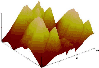
Figure 3. AFM image of a screw dislocation on a (0001) facet on the as-grown surface of AlN
Epitaxial Growth on A-Face Substrates
Boules of AlN have been cut to obtain several c-face and a-face substrates. Due to the extreme hardness of AlN, preparing high quality surfaces by common mechanical polishing process is both time-consuming and difficult. Mechanical polishing using diamond powder was not successful in obtaining an adequate surface for epitaxial growth as reported in a previous work [Reference Schowalter, Rojo, Slack, Shusterman, Wang, Bhat and Arunmozhi2]. Chemical-Mechanical Polishing (CMP) was, however, very successful in achieving epitaxial-growth-quality surfaces. Examination of the substrate by AFM showed a nearly atomically flat surface with monolayer steps and with all evidence of mechanical damage (sawing damage, scratches, etc.) removed. Rutherford backscattering/ion channeling (RBS) spectra were used to determine the crystal quality of the substrate surface and the grown epitaxial layers. The minimum yield χmin is used as a measure of the crystal quality and is defined as the ratio between the backscattered ion yield when the incident beam is aligned along a particular crystallographic axis and the backscattered ion yield when the incident beam is aligned randomly (along some non-crystallographic direction). The χmin will increase with increasing defect density. We have measured χmin in the spectral window corresponding to ion scattering from immediately below the sample surface peak. The results (see figure 4) show a χmin’s of 1.4% along the [11

Figure 4. Ion-channeling results obtained on the a-face after CMP process
Determination of the Etching Effects on Vicinal C-Faces
Several studies performed on polycrystalline AlN have shown high etch rates obtain by using KOH based solutions. However, very little work has been done on etching of AlN single crystals. Recently, Mileham et al. [Reference Mileham, Pearton, Abernathy, MacKenzie, Shul and Kilcoyne3] reported the first etching study on AlN single crystal grown on Al2O3. It was found that the etching rate depends critically on the crystalline quality and that the etching process is much faster at the grain boundary or wherever the density of defects is higher. Nevertheless, those crystal layers were defective and they do not report any orientation-dependent etching effect. The production of large, high-quality AlN single crystal substrates has made it possible to perform a more detailed study on the effect of KOH-based solutions on this material and to distinguish the differences of the etching process on different crystal orientations.
During the preparation of a vicinal c-face substrate (cut 20° off axis), we observed that cleaning the substrate with a phosphoric/sulfuric acid mixture gave different results for the two sides of the substrate. One side, which turned out to be the N-terminated face, became very rough surface. When a substrate with the same orientation was submerged in 1:2.5 KOH:water (by weight) solution for 3 minutes, AFM observation of the sample revealed the same unequal result for each side of the substrate. However, the KOH solution resulted in a slower etching rate than that produced by the phosphoric acid. AFM imaging (see figure 5) revealed a surface consisting of pyramids with a height between 0.5 and 1.5 μm high. This surface cannot be considered adequate for epitaxial growth. However, on the side that turned out to be the Al-terminated face the etching rate was unobservable resulting in a flatter surface.

Figure 5. AFM image on a 2x2 μm2 area of the N-terminated c-face of AlN after KOH etching. Each height division represents 0.5 μm
Study of the Surface Polarity by Tem
In order to identify the atomic termination of the side that resulted in a larger etching effect on the vicinal c-face of our substrate, a TEM-based method was used. Transmission electron microscopy (TEM) was carried out using JEOL 2010 and JEOL 200CX operated at 200 kV. We used a conventional TEM sample preparation technique consisting of mechanical polishing followed by Ar+ ion milling of the specimen. The MacTempas© program was used for calculations of the diffracted beam intensities. Large, electron-transparent areas of the crystal were studied by TEM using different sets of two-beam, bright-field/dark-field conditions. The imaging was done close to [ 11

Figure 6. Typical TEM image of the crystal taken under g= 10

Figure 7. Selected area electron diffraction pattern of the AlN crystal taken from the area of about 1.5 μm in diameter ([ 11
We have studied the polarity of the crystal surfaces using the method described by Dovidenko et al. [Reference Dovidenko, Oktyabrsky, Narayan and Razeghi4]. The method is based on the specific dependence of diffracted beam intensity vs. specimen thickness for the diffracted beams revealing the non-centrosymmetric nature of the crystal structure. We have carried out calculation of the intensities of different diffracted beams for the [ 11

Figure 9. Calculated intensities (arbitrary units) of the 0002, 000

Figure 9. Convergent beam electron diffraction pattern taken from the thin (about 100 Å) region of the AlN crystal in [ 11
Conclusions
We have demonstrated the growth of large AlN boules with low-dislocation-density, single-crystal grains. High quality a-face AlN substrates have been prepared using a chemical-mechanical polishing technique. High quality epitaxial layers of AlN and AlGaN have been grown on substrates of this orientation without the need for buffer layers. Finally, we have reported the different morphology and behavior after KOH and phosphoric acid etching on the N and Al-terminated faces along the c-axis. The identification of these faces has been carried out with convergent beam electron diffraction.
Acknowledgements
Financial support from ONR, BMDO, and the US Navy is acknowledged as well as the support of our contract monitors Dr. C.E.C. Wood (ONR), Dr. C. Litton (AFRL), and T. Groshens (Naval Surface Warfare Center).