Hostname: page-component-cd9895bd7-lnqnp Total loading time: 0 Render date: 2025-01-03T15:57:12.554Z Has data issue: false hasContentIssue false

Texture size control by mixing glass microparticles with alkaline solution for crystalline silicon solar cells

Published online by Cambridge University Press:  12 June 2018

Cong Thanh Nguyen*
Affiliation:
Center for Nano Materials and Technology (CNMT), Japan Advanced Institute of Science and Technology (JAIST), Nomi, Ishikawa 923-1292, Japan
Koichi Koyama
Affiliation:
Center for Nano Materials and Technology (CNMT), Japan Advanced Institute of Science and Technology (JAIST), Nomi, Ishikawa 923-1292, Japan
Huynh Thi Cam Tu
Affiliation:
Center for Nano Materials and Technology (CNMT), Japan Advanced Institute of Science and Technology (JAIST), Nomi, Ishikawa 923-1292, Japan
Keisuke Ohdaira
Affiliation:
Center for Nano Materials and Technology (CNMT), Japan Advanced Institute of Science and Technology (JAIST), Nomi, Ishikawa 923-1292, Japan
Hideki Matsumura*
Affiliation:
Center for Nano Materials and Technology (CNMT), Japan Advanced Institute of Science and Technology (JAIST), Nomi, Ishikawa 923-1292, Japan
*
a)Address all correspondence to these authors. e-mail: [email protected]
Get access

Abstract

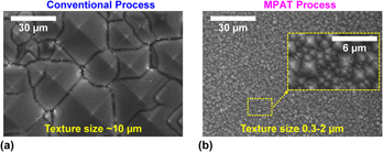
In this paper, we show a novel method to obtain small size textures usable in crystalline silicon (c-Si) solar cells. SiO2-based glass microparticles are mixed with a conventional KOH-based alkaline solution for making the textures. Using this mixing method, the texture size can be drastically reduced from 10 to ≤2 µm (0.3–2 µm). In addition, the process time and c-Si loss during the texture formation are reduced from 25 to 2 min and from 20 to 2 µm, respectively. Thus, the process is applicable to c-Si with thickness down to 50 µm. High-quality passivation showing the effective minority carrier lifetimes (τeff) larger than several ms and effective antireflection coating are possible on the new textures. The process is named “microparticle-assisted texturing (MPAT) process”, and its features are also demonstrated.

Type
Invited Feature Paper
Copyright
Copyright © Materials Research Society 2018 

Access options

Get access to the full version of this content by using one of the access options below. (Log in options will check for institutional or personal access. Content may require purchase if you do not have access.)

Footnotes

c)

Present address: ULVAC, Inc. (ULVAC), Chigasaki, Kanagawa 253-8543, Japan.

This paper has been selected as an Invited Feature Paper.

References

REFERENCES

Yoshikawa, K., Kawasaki, H., Yoshida, W., Irie, T., Konishi, K., Nakano, K., Uto, T., Adachi, D., Kanematsu, M., Uzu, H., and Yamamoto, K.: Silicon heterojunction solar cell with interdigitated back contacts for a photoconversion efficiency over 26%. Nat. Energy 2, 17032 (2017).Google Scholar
Jansen, H., de Boer, M., Legtenberg, R., and Elwenspoek, M.: The black silicon method: A universal method for determining the parameter setting of a fluorine-based reactive ion etcher in deep silicon trench etching with profile control. J. Micromech. Microeng. 5, 115 (1995).CrossRefGoogle Scholar
Kumaravelu, G., Alkaisi, M.M., Bittar, A., Macdonald, D., and Zhao, J.: Damage studies in dry etched textured silicon surfaces. Curr. Appl. Phys. 4, 108 (2004).CrossRefGoogle Scholar
Nguyen, C.T., Koyama, K., Terashima, S., Okamoto, C., Sugiyama, S., Ohdaira, K., and Matsumura, H.: 43rd IEEE Photovoltaic Specialists Conference (IEEE, Portland, OR, 2016).Google Scholar
Nguyen, C.T., Koyama, K., Higashimine, K., Terashima, S., Okamoto, C., Sugiyama, S., Ohdaira, K., and Matsumura, H.: Novel chemical cleaning of textured crystalline silicon for realizing surface recombination velocity <0.2 cm/s using passivation catalytic CVD SiNx/amorphous silicon stacked layers. Jpn. J. Appl. Phys. 56, 56502 (2017).Google Scholar
Koyama, K., Ohdaira, K., and Matsumura, H.: Extremely low surface recombination velocities on crystalline silicon wafers realized by catalytic chemical vapor deposited SiNx/a-Si stacked passivation layers. Appl. Phys. Lett. 97, 82108 (2010).CrossRefGoogle Scholar
Seidel, H., Csepregi, L., Heuberger, A., and Baumgärtel, H.: Anisotropic etching of crystalline silicon in alkaline solutions. J. Electrochem. Soc. 137, 3612 (1990).Google Scholar