Hostname: page-component-cd9895bd7-dk4vv Total loading time: 0 Render date: 2024-12-19T07:54:16.081Z Has data issue: false hasContentIssue false

Surface states in a monolayer MoS2 transistor

Published online by Cambridge University Press:  26 January 2016

Zhongyuan Lu
Affiliation:
Department of Electrical Engineering and Computer Sciences, University of California, Berkeley, California 94720, USA
Oukjae Lee
Affiliation:
Department of Electrical Engineering and Computer Sciences, University of California, Berkeley, California 94720, USA
Justin C. Wong
Affiliation:
Department of Electrical Engineering and Computer Sciences, University of California, Berkeley, California 94720, USA
Sayeef Salahuddin*
Affiliation:
Department of Electrical Engineering and Computer Sciences, University of California, Berkeley, California 94720, USA
*
a) Address all correspondence to this author. e-mail: [email protected]
Get access

Abstract

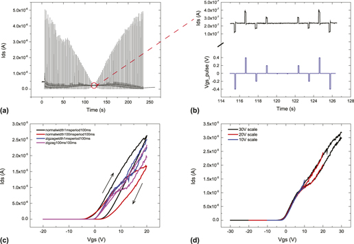
In this article, we have explored the interface states that form between the channel of a monolayer MoS2 transistor and a high-κ gate dielectric. These interface states lead to large hysteresis in the drain current versus gate voltage characteristic or the so-called transfer characteristic of the transistor. By applying carefully designed pulses to the gate of the transistor, we show that it is possible to both understand the nature of the interface states and minimize the hysteresis, so that the transfer characteristic can be reliably used for subsequent extraction of material parameters such as mobility.

Type
Invited Articles
Copyright
Copyright © Materials Research Society 2016 

Access options

Get access to the full version of this content by using one of the access options below. (Log in options will check for institutional or personal access. Content may require purchase if you do not have access.)

References

REFERENCES

Wang, Q.H., Kalantar-Zadeh, K., Kis, A., Coleman, J.N., and Strano, M.S.: Electronics and optoelectronics of two-dimensional transition metal dichalcogenides. Nat. Nanotechnol. 7(11), 699712 (2012).CrossRefGoogle ScholarPubMed
Novoselov, K.S., Geim, A.K., Morozov, S.V., Jiang, D., Zhang, Y., Dubonos, S.V., Grigorieva, I.V., and Firsov, A.A.: Electric field effect in atomically thin carbon films. Science 306(5696), 666669 (2004).CrossRefGoogle ScholarPubMed
Mak, K.F., Lee, C., Hone, J., Shan, J., and Heinz, T.F.: Atomically thin MoS2: A new direct-gap semiconductor. Phys. Rev. Lett. 105(13), 136805 (2010).CrossRefGoogle ScholarPubMed
Cao, T., Wang, G., Han, W., Ye, H., Zhu, C., Shi, J., and Niu, Q.: Valley-selective circular dichroism of monolayer molybdenum disulphide. Nat. Commun. 3, 887 (2012).CrossRefGoogle ScholarPubMed
Liu, H., Neal, A.T., and Ye, P.D.: Channel length scaling of MoS2 MOSFETs. ACS Nano 6(10), 85638569 (2012).CrossRefGoogle ScholarPubMed
Yoon, Y., Ganapathi, K., and Salahuddin, S.: How good can monolayer MoS2 transistors be?. Nano Lett. 11(9), 37683773 (2011).CrossRefGoogle Scholar
Radisavljevic, B., Radenovic, A., Brivio, J., Giacometti, V., and Kis, A.: Single-layer MoS2 transistors. Nat. Nanotechnol. 6(3), 147150 (2011).CrossRefGoogle ScholarPubMed
Kim, S., Konar, A., Hwang, W.S., Lee, J.H., Lee, J., Yang, J., and Jung, C.: High-mobility and low-power thin-film transistors based on multilayer MoS2 crystals. Nat. Commun. 3, 1011 (2012).CrossRefGoogle ScholarPubMed
Perera, M.M., Lin, M.W., Chuang, H.J., Chamlagain, B.P., Wang, C., Tan, X., Cheng, M.M.C., Tománek, D., and Zhou, Z.: Improved carrier mobility in few-layer MoS2 field-effect transistors with ionic-liquid gating. ACS Nano 7(5), 44494458 (2013).CrossRefGoogle ScholarPubMed
Das, S., Chen, H.Y., Penumatcha, A.V., and Appenzeller, J.: High performance multilayer MoS2 transistors with scandium contacts. Nano Lett. 13(1), 100105 (2012).CrossRefGoogle ScholarPubMed
Chang, H.Y., Yang, S., Lee, J., Taom, L., Hwang, W.-S., Jena, D., Lu, N., and Akinwande, D.: High-performance, highly bendable MoS2 transistors with high-k dielectrics for flexible low-power systems. ACS Nano 7(6), 54465452 (2013).CrossRefGoogle ScholarPubMed
Late, D.J., Liu, B., Matte, H.S.S.R., Dravid, V.P., and Rao, C.N.R.: Hysteresis in single-layer MoS2 field effect transistors. ACS Nano 6(6), 56355641 (2012).CrossRefGoogle ScholarPubMed
Li, T., Du, G., Zhang, B., and Zeng, Z.: Scaling behavior of hysteresis in multilayer MoS2 field effect transistors. Appl. Phys. Lett. 105(9), 093107 (2014).CrossRefGoogle Scholar
Ghatak, S., Pal, A.N., and Ghosh, A.: Nature of electronic states in atomically thin MoS2 field-effect transistors. ACS Nano 5(10), 77077712 (2011).CrossRefGoogle ScholarPubMed
Guo, Y., Wei, X., Shu, J., Liu, B., Yin, J., Guan, C., Han, Y., Gao, S., and Chen, Q.: Charge trapping at the MoS2–SiO2 interface and its effects on the characteristics of MoS2 metal-oxide-semiconductor field effect transistors. Appl. Phys. Lett. 106(10): 103109 (2015).CrossRefGoogle Scholar
Cho, K., Park, W., Park, J., Jeong, H., Jang, J., Kim, T.-Y., Hong, W.-K., Hong, S., and Lee, T.: Electric stress-induced threshold voltage instability of multilayer MoS2 field effect transistors. ACS Nano 7(9), 77517758 (2013).CrossRefGoogle ScholarPubMed
Lee, G.H., Yu, Y.J., Cui, X., Petrone, N., Lee, C.-H., Choi, M.S., and Lee, D.-Y.: Flexible and transparent MoS2 field-effect transistors on hexagonal boron nitride-graphene heterostructures. ACS Nano 7(9), 79317936 (2013).CrossRefGoogle ScholarPubMed
Benameur, M.M., Radisavljevic, B., Heron, J.S., Sahoo, S., Berger, H., and Kis, A.: Visibility of dichalcogenide nanolayers. Nanotechnology 22(12), 125706 (2011).CrossRefGoogle ScholarPubMed
Liu, W., Kang, J., Sarkar, D., Khatami, Y., Jena, D., and Banerjee, K.: Role of metal contacts in designing high-performance monolayer n-type WSe2 field effect transistors. Nano Lett. 13(5), 19831990 (2013).CrossRefGoogle ScholarPubMed
Taur, Y. and Ning, T.H.: Fundamentals of Modern VLSI Devices (Cambridge University Press, New York, 2009).CrossRefGoogle Scholar
Choi, K., Raza, S.R.A., Lee, H.S., Jeon, P.J., Pezeshki, A., Min, S.-W., and Kim, J.S.: Trap density probing on top-gate MoS2 nanosheet field-effect transistors by photo-excited charge collection spectroscopy. Nanoscale 7(13), 56175623 (2015).CrossRefGoogle ScholarPubMed
Estrada, D., Dutta, S., Liao, A., and Pop, E.: Reduction of hysteresis for carbon nanotube mobility measurements using pulsed characterization. Nanotechnology 21(8), 085702 (2010).CrossRefGoogle ScholarPubMed
Mattmann, M., Roman, C., Helbling, T., Bechstein, D., Durrer, L., Pohle, R., Fleischer, M., and Hierold, C.: Pulsed gate sweep strategies for hysteresis reduction in carbon nanotube transistors for low concentration NO2 gas detection. Nanotechnology 21(18), 185501 (2010).CrossRefGoogle Scholar
Liu, Z., Qiu, Z.J., Zhang, Z.B., Zheng, L.-R., and Zhang, S.-L.: Mobility extraction for nanotube TFTs. IEEE Electron Device Lett. 32(7), 913915 2011.CrossRefGoogle Scholar