Hostname: page-component-78c5997874-ndw9j Total loading time: 0 Render date: 2024-11-16T15:32:43.892Z Has data issue: false hasContentIssue false

Structural and multiband photoluminescent properties of a hierarchical ZnO/Si nanoheterostructure

Published online by Cambridge University Press:  26 April 2011

Hai Jun Xu*
Affiliation:
State Key Laboratory of Chemical Resource Engineering and School of Science, Beijing University of Chemical Technology, Beijing 100029, People’s Republic of China
Lei Su
Affiliation:
State Key Laboratory of Chemical Resource Engineering and School of Science, Beijing University of Chemical Technology, Beijing 100029, People’s Republic of China
Yu Fei Chan
Affiliation:
State Key Laboratory of Chemical Resource Engineering and School of Science, Beijing University of Chemical Technology, Beijing 100029, People’s Republic of China
Xiao Ming Sun
Affiliation:
State Key Laboratory of Chemical Resource Engineering and School of Science, Beijing University of Chemical Technology, Beijing 100029, People’s Republic of China
*
a)Address all correspondence to this author. e-mail: [email protected]
Get access

Abstract

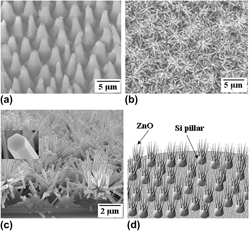
Hierarchical ZnO/Si nanoheterostructure was prepared by growing oriented ZnO nanowire bundles onto the top of nanoporous silicon pillar array (NSPA) via a self-catalytic thermal evaporation and vapor-phase transport method. Samples were carefully characterized using field emission scanning electron microscopy, x-ray diffraction, and luminescence spectroscopy. One ultraviolet, one blue-green, and two red emission bands were observed in ZnO/NSPA, and the emission mechanism is discussed by developing a model-based energy band diagram. The origins of the ultraviolet and blue-green photoluminescence (PL) bands were attributed to the emission from the band edge transition and surface states of oxygen vacancies of ZnO, while two red PL bands originated from NSPA and could be well explained by the quantum confinement-luminescence center model. The realization of such all solid and wide wavelength nanodevice might be both meaningful for developing new concept lighting devices and potentially extended to fabricate hierarchical Si-based nanoheterostructures in fabricating other optoelectronic nanodevices.

Type
Articles
Copyright
Copyright © Materials Research Society 2011

Access options

Get access to the full version of this content by using one of the access options below. (Log in options will check for institutional or personal access. Content may require purchase if you do not have access.)

References

REFERENCES

1.Rohrmoser, S., Baldauf, J., Harley, R.T., Lagoudakis, P.G., Sapra, S., and Eychmuller, A.: Temperature dependence of exciton transfer in hybrid quantum well/nanocrystal heterostructures. Appl. Phys. Lett. 91, 092126 (2007).Google Scholar
2.Xiang, J., Lu, W., Hu, Y., Wu, Y., Yan, H., and Lieber, C.M.: Ge/Si nanowire heterostructures as high-performance field-effect transistors. Nature 441, 489 (2006).CrossRefGoogle ScholarPubMed
3.Rauter, P., Fromherz, T., Vinh, N.Q., Murdin, B.N., Mussler, G., Grutzmacher, D., and Bauer, G.: Continuous voltage tunability of intersubband relaxation times in coupled SiGe quantum well structures using ultrafast spectroscopy. Phys. Rev. Lett. 102, 147401 (2009).CrossRefGoogle ScholarPubMed
4.Long, H., Fang, G., Huang, H., Mo, X., Xia, W., Dong, B., Meng, X., and Zhao, X.: Ultraviolet electroluminescence from ZnO/NiO-based heterojunction light-emitting diodes. Appl. Phys. Lett. 95, 013509 (2009).CrossRefGoogle Scholar
5.Tzolov, M., Chang, B., Yin, A., Straus, D., Xu, J.M., and Brown, G.: Electronic transport in a controllably grown carbon nanotube-silicon heterojunction array. Phys. Rev. Lett. 92, 075505 (2004).CrossRefGoogle Scholar
6.Yi, W., Narayanamurti, V., Lu, H., Scarpulla, M.A., and Gossard, C.: Probing semiconductor band structures and heterojunction interface properties with ballistic carrier emission: GaAs/AlxGa1−xAs as a model system. Phys. Rev. B 81, 235325 (2010).Google Scholar
7.Jeong, M.C., Oh, B.Y., Ham, M.H., Lee, S.W., and Myoung, J.M.: ZnO-nanowire-inserted GaN/ZnO heterojunction light-emitting diodes. Small 3, 568 (2007).CrossRefGoogle ScholarPubMed
8.Tak, Y., Hong, J., Lee, J.S., and Yong, K.: Fabrication of ZnO/CdS core/shell nanowire arrays for efficient solar energy conversion. J. Mater. Chem. 19, 5945 (2009).Google Scholar
9.Hsieh, Y., Chen, H., Lin, M., Shiu, S., Hofmann, M., Chern, M., Jia, X., Yang, Y., Chang, H., Huang, H., Tseng, S., Chen, L., Chen, K., Lin, C., Liang, C., and Chen, Y.: Electroluminescence from ZnO/Si-nanotips light-emitting diodes. Nano Lett. 9, 1839 (2009).CrossRefGoogle ScholarPubMed
10.Willander, M., Nur, O., Bano, N., and Sultana, K.: Zinc oxide nanorod-based heterostructures on solid and soft substrates for white-light-emitting diode applications. N. J. Phys. 11, 125020 (2009).CrossRefGoogle Scholar
11.Chang, Y.M., Jian, S.R., Lee, H.Y., Lin, C.M., and Juang, J.Y.: Enhanced visible photoluminescence from ultrathin ZnO films grown on Si-nanowires by atomic layer deposition. Nanotechnology 21, 385705 (2010).Google Scholar
12.Xu, H.J. and Li, X.J.: Silicon nanoporous pillar array: A silicon hierarchical structure with high light absorption and triple-band photoluminescence. Opt. Express 16, 2933 (2008).Google Scholar
13.Xu, H.J. and Li, X.J.: Preparation, structural and photoluminescent properties of CdS/silicon nanoporous pillar array. J. Phys. Condens. Matter 19, 056003 (2007).CrossRefGoogle Scholar
14.Xu, H.J. and Li, X.J.: Rectification effect and electron transport property of CdS/Si nanoheterostructure based on silicon nanoporous pillar array. Appl. Phys. Lett. 93, 172105 (2008).CrossRefGoogle Scholar
15.Yan, X., Tay, B.K., and Miele, P.: Field emission from ordered carbon nanotube-ZnO heterojunction arrays. Carbon 46, 753 (2008).CrossRefGoogle Scholar
16.Fan, Z., Ruebusch, D.J., Rathore, A.J., Kapadia, R., Ergen, O., Leu, P.W., and Javey, A.: Challenges and prospects of nanopillar based solar cells. Nano Res. 2, 829 (2009).CrossRefGoogle Scholar
17.Ku, C.S., Huang, J.M., Cheng, C.Y., Lin, C.M., and Lee, H.Y.: Annealing effect on the optical response and interdiffusion of n-ZnO/p-Si (111) heterojunction grown by atomic layer deposition. Appl. Phys. Lett. 97, 181915 (2010).CrossRefGoogle Scholar
18.Fonoberov, V.A., Alim, K.A., Balandin, A.A., Xiu, F.X., and Liu, J.L.: Competition between exciton-phonon interaction and defects states in the 3.31 eV band in ZnO. Phys. Rev. B. 73, 165317 (2006).CrossRefGoogle Scholar
19.Li, C., Fang, G.J., Su, G.H., Li, G.H., Wu, X.G., and Zhao, X.Z.: Synthesis and photoluminescence properties of vertically aligned ZnO nanorod-nanowall junction arrays on a ZnO-coated silicon substrate. Nanotechnology 17, 3740 (2006).CrossRefGoogle Scholar
20.Kasai, P.H.: Electron spin resonance studies of donors and acceptors in ZnO. Phys. Rev. 130, 989 (1963).CrossRefGoogle Scholar
21.Dijken, A.V., Meulenkamp, E.A., Vanmaekelbergh, D., and Meijerink, A.: The kinetics of the radiative and nonradiative processes in nanocrystalline ZnO particles upon photoexcitation. J. Phys. Chem. B 104, 1715 (2000).CrossRefGoogle Scholar
22.Liu, Y.L., Liu, Y.C., Yang, H., Wang, W.B., Ma, J.G., Zhang, J.Y., Lu, Y.M., Shen, D.Z., and Fan, X.W.: The optical properties of ZnO films grown on porous Si templates. J. Phys. D Appl. Phys. 36, 2705 (2003).CrossRefGoogle Scholar
23.Singh, R.G., Singh, F., Kanjilal, D., Agarwal, V., and Mehra, R.M.: White light emission from chemically synthesized ZnO–porous silicon nanocomposite. J. Phys. D Appl. Phys. 42, 062002 (2009).CrossRefGoogle Scholar