Hostname: page-component-78c5997874-8bhkd Total loading time: 0 Render date: 2024-11-16T13:21:58.756Z Has data issue: false hasContentIssue false

Stress relaxation and failure behavior of Sn–3.0Ag–0.5Cu flip-chip solder bumps undergoing electromigration

Published online by Cambridge University Press:  08 September 2014

Mingliang Huang*
Affiliation:
Electronic Packaging Materials Laboratory, School of Materials Science & Engineering, Dalian University of Technology, Dalian 116024, People's Republic of China
Zhijie Zhang
Affiliation:
Electronic Packaging Materials Laboratory, School of Materials Science & Engineering, Dalian University of Technology, Dalian 116024, People's Republic of China
Shaoming Zhou
Affiliation:
Electronic Packaging Materials Laboratory, School of Materials Science & Engineering, Dalian University of Technology, Dalian 116024, People's Republic of China
Leida Chen
Affiliation:
Electronic Packaging Materials Laboratory, School of Materials Science & Engineering, Dalian University of Technology, Dalian 116024, People's Republic of China
*
a)Address all correspondence to this author. e-mail: [email protected]
Get access

Abstract

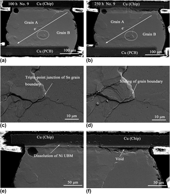
The stress relaxation and failure behavior of Ni/Sn–3.0Ag–0.5Cu/electroless nickel electroless palladium immersion gold flip-chip solder bumps undergoing electromigration (EM) at 150 °C under 1.5 × 10⁴ A/cm2 was investigated in situ. Three modes of stress relaxation of Sn–3.0Ag–0.5Cu solder bumps were identified. At the cathode, voids and hollows with terrace morphology gradually formed to relieve the tensile stress; at the anode, especially around the current crowding corner, recrystallization of Sn grains and extrusion of hillocks occurred to relieve the compressive stress; in the solder bump, Sn grain boundary sliding that occurred to accommodate the diffusion creep was more pronounced with increasing EM time. Grain boundary sliding is considered to be an indispensable requisite for diffusion creep. The microstructural evolution of solder bumps at the last stage of lifetime was revealed, and the final EM-induced failure mode was the local fusion of a solder bump resulting from the crack formation-and-propagation at the cathode.

Type
Articles
Copyright
Copyright © Materials Research Society 2014 

Access options

Get access to the full version of this content by using one of the access options below. (Log in options will check for institutional or personal access. Content may require purchase if you do not have access.)

References

REFERENCES

Chen, C., Tong, H.M., and Tu, K.N.: Electromigration and thermomigration in Pb-free flip-chip solder joints. Annu. Rev. Mater. Res. 40, 531 (2010).CrossRefGoogle Scholar
Chan, Y.C. and Yang, D.: Failure mechanisms of solder interconnects under current stressing in advanced electronic packages. Prog. Mater. Sci. 55, 428 (2010).Google Scholar
Blech, I.A.: Electromigration in thin aluminum films on titanium nitride. J. Appl. Phys. 47, 1203 (1976).Google Scholar
Xu, L.H., Pang, J.H.L., and Tu, K.N.: Effect of electromigration-induced back stress gradient on nanoindentation marker movement in SnAgCu solder joints. Appl. Phys. Lett. 89, 221909 (2006).Google Scholar
Ouyang, F.Y., Chen, K., Tu, K.N., and Lai, Y.S.: Effect of current crowding on whisker growth at the anode in flip chip solder joints. Appl. Phys. Lett. 91, 231919 (2007).CrossRefGoogle Scholar
Zhu, Q.S., Liu, H.Y., Wang, Z.G., and Shang, J.K.: Surface morphology of Sn-rich solder interconnects after electrical loading. J. Electron. Mater. 41, 741 (2012).CrossRefGoogle Scholar
Lin, Y.H., Hu, Y.C., Tsai, C.M., Kao, C.R., and Tu, K.N.: In situ observation of the void formation-and-propagation mechanism in solder joints under current-stressing. Acta Mater. 53, 2029 (2005).Google Scholar
Jen, M.H.R., Liu, L.C., and Lai, Y.S.: Electromigration on void formation of Sn3Ag1.5Cu FCBGA solder joints. Microelectron. Reliab. 49, 734 (2009).CrossRefGoogle Scholar
Huang, M.L., Ye, S., and Zhao, N.: Current-induced interfacial reactions in Ni/Sn-3Ag-0.5Cu/Au/Pd(P)/Ni-P flip chip interconnect. J. Mater. Res. 26, 3009 (2011).Google Scholar
Law, C.M.T., Wu, C.M.L., Yu, D.Q., Li, M., and Chi, D.Z.: Interfacial microstructure and strength of lead-free Sn-Zn-RE BGA solder bumps. IEEE Trans. Adv. Packag. 28, 252 (2005).CrossRefGoogle Scholar
Zhang, L.Y., Ou, S.Q., Huang, J., Tu, K.N., Gee, S., and Nguyen, L.: Effect of current crowding on void propagation at the interface between intermetallic compound and solder in flip chip solder joints. Appl. Phys. Lett. 88, 012106 (2006).Google Scholar
Yeh, E.C.C., Choi, W.J., Tu, K.N., Elenius, P., and Balkan, H.: Current-crowding-induced electromigration failure in flip chip solder joints. Appl. Phys. Lett. 80, 580 (2002).Google Scholar
Herring, C.: Diffusional viscosity of a polycrystalline solid. J. Appl. Phys. 21, 437 (1950).Google Scholar
Coble, R.L.: A model for boundary diffusion controlled creep in polycrystalline materials. J. Appl. Phys. 34, 1679 (1963).CrossRefGoogle Scholar
Lu, M.H., Shih, D.Y., Lauro, P., Goldsmith, C., and Henderson, D.W.: Effect of Sn grain orientation on electromigration degradation mechanism in high Sn-based Pb-free solders. Appl. Phys. Lett. 92, 211909 (2008).CrossRefGoogle Scholar
Wu, A.T., Gusak, A.M., and Tu, K.N.: Electromigration-induced grain rotation in anisotropic conducting beta tin. Appl. Phys. Lett. 86, 241902 (2005).Google Scholar
Lee, A., Liu, W., Ho, C.E., and Subramanian, K.N.: Synchrotron x-ray microscopy studies on electromigration of a two-phase material. J. Appl. Phys. 102, 053507 (2007).CrossRefGoogle Scholar
Ke, J.H., Yang, T.L., Lai, Y.S., and Kao, C.R.: Analysis and experimental verification of the competing degradation mechanisms for solder joints under electron current stressing. Acta Mater. 59, 2462 (2011).Google Scholar
Chen, S.W., Lin, S.K., and Jao, J.M.: Electromigration effects upon interfacial reactions in flip-chip solder joints. Mater. Trans. 45, 661 (2004).Google Scholar
Wei, C.C. and Chen, C.: Critical length of electromigration for eutectic SnPb solder stripe. Appl. Phys. Lett. 88, 182105 (2006).Google Scholar