Hostname: page-component-cd9895bd7-mkpzs Total loading time: 0 Render date: 2024-12-28T13:50:28.292Z Has data issue: false hasContentIssue false

Multidimensional SPM applied for nanoscale conductance mapping

Published online by Cambridge University Press:  20 December 2013

James L. Bosse
Affiliation:
Department of Materials Science and Engineering, University of Connecticut, Storrs, Connecticut 06269-3136
Ilja Grishin
Affiliation:
Department of Physics, Lancaster University, Lancaster LA1 4YB, United Kingdom
Oleg V. Kolosov
Affiliation:
Department of Physics, Lancaster University, Lancaster LA1 4YB, United Kingdom
Bryan D. Huey*
Affiliation:
Department of Materials Science and Engineering, University of Connecticut, Storrs, Connecticut 06269-3136
*
a)Address all correspondence to this author. e-mail: [email protected]
Get access

Abstract

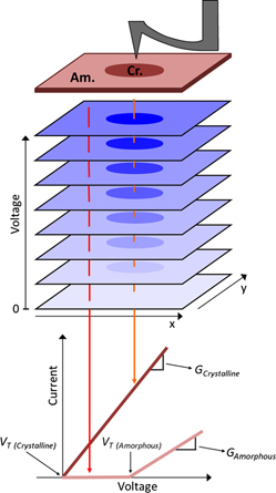
A new approach has been developed for nanoscale conductance mapping (NCM) based on multidimensional atomic force microscopy (AFM) to efficiently investigate the nanoscale electronic properties of heterogeneous surfaces. The technique uses a sequence of conductive AFM images, all acquired in a single area but each with incrementally higher applied voltages. This generates a matrix of current versus voltage (IV) spectra, providing nanoscale maps of conductance and current nonlinearities with negligible spatial drift. For crystalline and amorphous phases of a GeSe chalcogenide phase change film, conductance and characteristic amorphous phase “turn-on” voltages are mapped with results providing traditional point-by-point IV measurements, but acquired hundreds of times faster. Although similar to current imaging tunneling spectroscopy in a scanning tunneling microscope, the NCM technique does not require conducting specimens. It is therefore a promising approach for efficient, quantitative electronic investigations of heterogeneous materials used in sensors, resistive memories, and photovoltaics.

Type
Articles
Copyright
Copyright © Materials Research Society 2013 

Access options

Get access to the full version of this content by using one of the access options below. (Log in options will check for institutional or personal access. Content may require purchase if you do not have access.)

References

REFERENCES

Binnig, G., Quate, C.F., and Gerber, C.: Atomic force microscope. Phys. Rev. Lett. 56(9), 930 (1986).CrossRefGoogle ScholarPubMed
Fiorenza, P., Lo Nigro, R., Raineri, V., and Salinas, D.: Breakdown kinetics at nanometer scale of innovative MOS devices by conductive atomic force microscopy. Microelectron. Eng. 84(3), 441 (2007).CrossRefGoogle Scholar
Dewolf, P., Snauwaert, J., Clarysse, T., Vandervorst, W., and Hellemans, L.: Characterization of a point-contact on silicon using force microscopy-supported resistance measurements. Appl. Phys. Lett. 66(12), 1530 (1995).CrossRefGoogle Scholar
Shafai, C., Thomson, D.J., Simardnormandin, M., Mattiussi, G., and Scanlon, P.J.: Delineation of semiconductor doping by scanning resistance microscopy. Appl. Phys. Lett. 64(3), 342 (1994).CrossRefGoogle Scholar
Chappanda, K.N. and Tabib-Azar, M.: Conducting AFM studies of metal surface contact resistance for NEMS switches. In Sensors, 2011 IEEE, edited by K. Ozanyan. (IEEE, New York, NY, 2011); p. 1371.CrossRefGoogle Scholar
Bayerl, A., Lanza, M., Porti, M., Campabadal, F., Nafria, M., Aymerich, X., and Benstetter, G.: Reliability and gate conduction variability of HfO2-based MOS devices: A combined nanoscale and device level study. Microelectron. Eng. 88(7), 1334 (2011).CrossRefGoogle Scholar
Moutinho, H.R., Dhere, R.G., Ballif, C., Al-Jassim, M.M., and Kazmerski, L.L.: Alternative procedure for the fabrication of close-spaced sublimated CdTe solar cells. J. Vac. Sci. Technol., A 18(4), 1599 (2000).CrossRefGoogle Scholar
Alperson, B., Cohen, S., Rubinstein, I., and Hodes, G.: Room-temperature conductance spectroscopy of CdSe quantum dots using a modified scanning force microscope. Phys. Rev. B 52(24), 17017 (1995).CrossRefGoogle ScholarPubMed
Leever, B.J., Durstock, M.F., Irwin, M.D., Hains, A.W., Marks, T.J., Pingree, L.S.C., and Hersam, M.C.: Spatially resolved photocurrent mapping of operating organic photovoltaic devices using atomic force photovoltaic microscopy. Appl. Phys. Lett. 92(1), 013302 (2008).CrossRefGoogle Scholar
Huey, B.D., Lisjak, D., and Bonnell, D.A.: Nanometer-scale variations in interface potential by scanning probe microscopy. J. Am. Ceram. Soc. 82(7), 1941 (1999).CrossRefGoogle Scholar
Huey, B.D. and Bonnell, D.A.: Nanoscale variation in electric potential at oxide bicrystal and polycrystal interfaces. Solid State Ionics 131(1–2), 51 (2000).CrossRefGoogle Scholar
Huey, B.D. and Bonnell, D.A.: Spatially localized dynamic properties of individual interfaces in semiconducting oxides. Appl. Phys. Lett. 76(8), 1012 (2000).CrossRefGoogle Scholar
Kim, H., Hong, S., and Kim, D-W.: Ambient effects on electric-field-induced local charge modification of TiO2. Appl. Phys. Lett. 100(2), (2012).Google Scholar
Ko, H., Ryu, K., Park, H., Park, C., Jeon, D., Kim, Y.K., Jung, J., Min, D-K., Kim, Y., Lee, H.N., Park, Y., Shin, H., and Hong, S.: High-resolution field effect sensing of ferroelectric charges. Nano Lett. 11(4), 1428 (2011).CrossRefGoogle ScholarPubMed
Bae, B.J., Hong, S.H., Hwang, S.Y., Hwang, J.Y., Yang, K.Y., and Lee, H.: Electrical characterization of Ge-Sb-Te phase change nano-pillars using conductive atomic force microscopy. Semicond. Sci. Technol. 24(7), 075016 (2009).CrossRefGoogle Scholar
Gidon, S., Lemonnier, O., Rolland, B., Bichet, O., Dressler, C., and Samson, Y.: Electrical probe storage using Joule heating in phase change media. Appl. Phys. Lett. 85(26), 6392 (2004).CrossRefGoogle Scholar
Gotoh, T., Sugawara, K., and Tanaka, K.: Minimal phase-change marks produced in amorphous Ge2Sb2Te5 films. Jpn. J. Appl. Phys. 43(6B), 818 (2004).CrossRefGoogle Scholar
Wong, H., Raoux, S., Kim, S., Liang, J., Reifenberg, J.P., Rajendran, B., Asheghi, M., and Goodson, K.E.: Phase change memory. Proc. IEEE 98(12), 2201 (2010).CrossRefGoogle Scholar
Wright, C.D., Armand, M., and Aziz, M.M.: Terabit-per-square-inch data storage using phase-change media and scanning electrical nanoprobes. IEEE Trans. Nanotechnol. 5(1), 50 (2006).CrossRefGoogle Scholar
Hamann, H.F., O'Boyle, M., Martin, Y.C., Rooks, M., and Wickramasinghe, K.: Ultra-high-density phase-change storage and memory. Nat. Mater. 5(5), 383 (2006).CrossRefGoogle ScholarPubMed
Klein, D.L. and Mceuen, P.L.: Conducting atomic-force microscopy of alkane layers on graphite. Appl. Phys. Lett. 66(19), 2478 (1995).CrossRefGoogle Scholar
Hauquier, F., Alamarguy, D., Viel, P., Noel, S., Filoramo, A., Huc, V., Houze, F., and Palacin, S.: Conductive-probe AFM characterization of graphene sheets bonded to gold surfaces. Appl. Surf. Sci. 258(7), 2920 (2012).CrossRefGoogle Scholar
Gosvami, N., Lau, K.H.A., Sinha, S.K., and O'Shea, S.J.: Effect of end groups on contact resistance of alkanethiol based metal-molecule-metal junctions using current sensing AFM. Appl. Surf. Sci. 252(11), 3956 (2006).CrossRefGoogle Scholar
Schloffer, M., Teichert, C., Supancic, P., Andreev, A., Hou, Y., and Wang, Z.H.: Electrical characterization of ZnO multilayer varistors on the nanometre scale with conductive atomic force microscopy. J. Eur. Ceram. Soc. 30(7), 1761 (2010).CrossRefGoogle Scholar
Lee, H.J., Lee, J., and Park, S.M.: Electrochemistry of conductive polymers. 45. Nanoscale conductivity of PEDOT and PEDOT: PSS composite films studied by current-sensing AFM. J. Phys. Chem. B 114(8), 2660 (2010).CrossRefGoogle ScholarPubMed
Bussian, D.A., O'Dea, J.R., Metiu, H., and Buratto, S.K.: Nanoscale current imaging of the conducting channels in proton exchange membrane fuel cells. Nano Lett. 7(2), 227 (2007).CrossRefGoogle ScholarPubMed
Alexeev, A., Loos, J., and Koetse, M.M.: Nanoscale electrical characterization of semiconducting polymer blends by conductive atomic force microscopy. Ultramicroscopy 106(3), 191 (2006).CrossRefGoogle ScholarPubMed
Kelley, T.W. and Frisbie, C.D.: Point contact current-voltage measurements on individual organic semiconductor grains by conducting probe atomic force microscopy. J. Vac. Sci. Technol., B 18(2), 632 (2000).CrossRefGoogle Scholar
Binnig, G., Rohrer, H., Gerber, C., and Weibel, E.: Surface studies by scanning tunneling microscopy. Phys. Rev. Lett. 49(1), 57 (1982).CrossRefGoogle Scholar
Salmeron, M., Ogletree, D.F., Ocal, C., Wang, H.C., Neubauer, G., Kolbe, W., and Meyers, G.: Tip-surface forces during imaging by scanning tunneling microscopy. J. Vac. Sci. Technol., B 9(2), 1347 (1991).CrossRefGoogle Scholar
Hersam, M.C., Hoole, A.C.F., O'Shea, S.J., and Welland, M.E.: Potentiometry and repair of electrically stressed nanowires using atomic force microscopy. Appl. Phys. Lett. 72(8), 915 (1998).CrossRefGoogle Scholar
Lin, H.N., Lin, H.L., Wang, S.S., Yu, L.S., Perng, G.Y., Chen, S.A., and Chen, S.H.: Nanoscale charge transport in an electroluminescent polymer investigated by conducting atomic force microscopy. Appl. Phys. Lett. 81(14), 2572 (2002).CrossRefGoogle Scholar
De Wolf, P., Stephenson, R., Trenkler, T., Clarysse, T., Hantschel, T., and Vandevorst, W.: Status and review of two-dimensional carrier and dopant profiling using scanning probe microscopy. J. Vac. Sci. Technol., B 18(1), 361 (2000).CrossRefGoogle Scholar
Moutinho, H.R., Dhere, R.G., Jiang, C.S., Al-Jassim, M.M., and Kazmerski, L.L.: Electrical properties of CdTe/CdS solar cells investigated with conductive atomic force microscopy. Thin Solid Films 514(1–2), 150 (2006).CrossRefGoogle Scholar
Otsuka, Y., Naitoh, Y., Matsumoto, T., and Kawai, T.: A nano tester: A new technique for nanoscale electrical characterization by point-contact current-imaging atomic force microscopy. Jpn. J. Appl. Phys., Part 2 41(7A), L742 (2002).CrossRefGoogle Scholar
Herruzo, E.T., Asakawa, H., Fukuma, T., and Garcia, R.: Three-dimensional quantitative force maps in liquid with 10 piconewton, angstrom and sub-minute resolutions. Nanoscale 5(7), 2678 (2013).CrossRefGoogle ScholarPubMed
Allers, W., Schwarz, A., Schwarz, U.D., and Wiesendanger, R.: A scanning force microscope with atomic resolution in ultrahigh vacuum and at low temperatures. Rev. Sci. Instrum. 69(1), 221 (1998).CrossRefGoogle Scholar
Albers, B.J., Liebmann, M., Schwendemann, T.C., Baykara, M.Z., Heyde, M., Salmeron, M., Altman, E.I., and Schwarz, U.D.: Combined low-temperature scanning tunneling/atomic force microscope for atomic resolution imaging and site-specific force spectroscopy. Rev. Sci. Instrum. 79(3), 033704 (2008).CrossRefGoogle ScholarPubMed
Baykara, M.Z., Schwendemann, T.C., Altman, E.I., and Schwarz, U.D.: Three-dimensional atomic force microscopy: Taking surface imaging to the next level. Adv. Mater. 22(26–27), 2838 (2010).CrossRefGoogle Scholar
Huey, B.D.: AFM and acoustics: Fast, quantitative nanomechanical mapping. Annu. Rev. Mater. Res. 37, 351 (2007).CrossRefGoogle Scholar
Bosse, J.L., Lee, S., Huey, B.D., Andersen, A.S., and Sutherland, D.S.: High speed friction microscopy and nanoscale friction coefficient mapping. Nanotechnology (2013, submitted).Google Scholar
Ho, W.: Single-molecule chemistry. J. Chem. Phys. 117(24), 11033 (2002).CrossRefGoogle Scholar
Jeong, D.S., Lim, H., Park, G.H., Hwang, C.S., Lee, S., and Cheong, B.K.: Threshold resistive and capacitive switching behavior in binary amorphous GeSe. J. Appl. Phys. 111(10), 102807 (2012).CrossRefGoogle Scholar
Picco, L.M., Bozec, L., Ulcinas, A., Engledew, D.J., Antognozzi, M., Horton, M.A., and Miles, M.J.: Breaking the speed limit with atomic force microscopy. Nanotechnology 18(4), 044030 (2007).CrossRefGoogle Scholar
Cowley, A.M.: Depletion capacitance and diffusion potential of gallium phosphide Schottky-barrier diodes. J. Appl. Phys. 37(8), 3024 (1966).CrossRefGoogle Scholar
Card, H. and Rhoderick, E.: Studies of tunnel MOS diodes I. Interface effects in silicon Schottky diodes. J. Phys. D: Appl. Phys. 4(10), 1589 (2002).CrossRefGoogle Scholar
Keenan, W., Schumann, P., Tong, A., and Phillips, R.: Ohmic Contacts to Semiconductors (The Electrochemical Society, Princeton, NJ, 1969).Google Scholar
Henisch, H.K.: Rectifying semiconductor contacts. J. Electrochem. Soc. 103(11), 637 (1956).CrossRefGoogle Scholar
Weisenhorn, A.L., Maivald, P., Butt, H.J., and Hansma, P.K.: Measuring adhesion, attraction, and repulsion between surfaces in liquids with an atomic-force microscope. Phys. Rev. B 45(19), 11226 (1992).CrossRefGoogle ScholarPubMed
Márquez, E., Nagels, P., González-Leal, J.M., Bernal-Oliva, A.M., Sleeckx, E., and Callaerts, R.: On the optical constants of amorphous GexSe1−x thin films of non-uniform thickness prepared by plasma-enhanced chemical vapour deposition. Vacuum 52(1–2), 55 (1999).CrossRefGoogle Scholar