Hostname: page-component-78c5997874-fbnjt Total loading time: 0 Render date: 2024-11-05T10:49:29.837Z Has data issue: false hasContentIssue false

Microstructure and thermoelectric properties of InSb compound with nonsoluble NiSb in situ precipitates

Published online by Cambridge University Press:  13 December 2013

Guangyu Jiang
Affiliation:
Department of Materials Science and Engineering, State Key Laboratory of Silicon Materials, Zhejiang University, Hangzhou 310027, People's Republic of China
Yi Chen
Affiliation:
Department of Materials Science and Engineering, State Key Laboratory of Silicon Materials, Zhejiang University, Hangzhou 310027, People's Republic of China
Tiejun Zhu
Affiliation:
Department of Materials Science and Engineering, State Key Laboratory of Silicon Materials, Zhejiang University, Hangzhou 310027, People's Republic of China; and Key Laboratory of Advanced Materials and Applications for Batteries of Zhejiang Province, Zhejiang University, Hangzhou 310027, China
Xiaohua Liu
Affiliation:
Department of Materials Science and Engineering, State Key Laboratory of Silicon Materials, Zhejiang University, Hangzhou 310027, People's Republic of China
Xinbing Zhao*
Affiliation:
Department of Materials Science and Engineering, State Key Laboratory of Silicon Materials, Zhejiang University, Hangzhou 310027, People's Republic of China; and Key Laboratory of Advanced Materials and Applications for Batteries of Zhejiang Province, Zhejiang University, Hangzhou 310027, China
*
a)Address all correspondence to this author. e-mail: [email protected]
Get access

Abstract

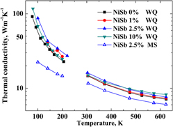
The microstructure and thermoelectric properties of InSb–NiSb composite system are investigated. NiSb, ranging from micro- to nanoscale, is introduced as a nonsoluble second phase in the InSb matrix by using the water quenching method. The morphology of the second phase is adjusted by varying the composition from hypoeutectic to hypereutectic alloys. The eutectic composite with a semiconducting InSb matrix and a metallic NiSb fiber on the order of 100-nm diameter is obtained. Melt spinning (MS) is applied to the eutectic composition to change the NiSb dispersion phase to around 200-nm diameter sphere. Transport properties, including Seebeck coefficient, resistivity, Hall coefficient, and thermal conductivity, are measured from 80 to 630 K. Compared to the water quenched (WQ) eutectic sample, the MS process results in a slight increase in the carrier concentration but a remarkable reduction in the mobility and thermal conductivity. Compared to the InSb matrix, ZT of the samples with the NiSb second phase is lower. For the eutectic samples, ZT is significantly reduced after the MS process because of the loss in mobility. ZT of the WQ InSb matrix is the highest in all the samples, ∼0.5 at 600 K.

Type
Articles
Copyright
Copyright © Materials Research Society 2013 

Access options

Get access to the full version of this content by using one of the access options below. (Log in options will check for institutional or personal access. Content may require purchase if you do not have access.)

References

REFERENCES

Rowe, D.M. and Bhandari, C.M.: Modern Thermoelectrics (Reston Publishing Company, Reston, VA, 1983).Google Scholar
Snyder, G.J. and Toberer, E.S.: Complex thermoelectric materials. Nat. Mater. 7(2), 105 (2008).CrossRefGoogle ScholarPubMed
Hu, L., Gao, H., Liu, X., Xie, H., Shen, J., Zhu, T., and Zhao, X.: Enhancement in thermoelectric performance of bismuth telluride based alloys by multi-scale microstructural effects. J. Mater. Chem. 22(32), 16484 (2012).CrossRefGoogle Scholar
Pei, Y., Wang, H., Gibbs, Z.M., LaLonde, A.D., and Snyder, G.J.: Thermopower enhancement in Pb1−xMnxTe alloys and its effect on thermoelectric efficiency. NPG Asia Mater. 4, e28 (2012).CrossRefGoogle Scholar
Shi, X., Yang, J., Salvador, J.R., Chi, M., Cho, J.Y., Wang, H., Bai, S., Yang, J., Zhang, W., and Chen, L.: Multiple-filled skutterudites: High thermoelectric figure of merit through separately optimizing electrical and thermal transports. J. Am. Chem. Soc. 133(20), 7837 (2011).CrossRefGoogle ScholarPubMed
Trifonov, V.I. and Yaremenko, N.G.: Deep Donor Level in InSb. Sov. Phys. Semicond. 5, 839 (1971).Google Scholar
Hrostowski, H.J., Morin, F.J., Geballe, T.H., and Wheatley, G.H.: Hall effect and conductivity of InSb. Phys. Rev. 100(6), 1672 (1955).CrossRefGoogle Scholar
Volokobinskaya, N.I., Galavanov, V.V., and Nasledov, D.N.: Sov. Phys. Solid State 1, 687 (1959).Google Scholar
Hishiki, S., Kanno, L., Sugiura, O., Xiang, R.F., Nakamura, T., and Katagiri, M.: Undoped InSb schottky detector for gamma-ray measurements. IEEE Trans. Nucl. Sci. 52(6), 3172 (2005).CrossRefGoogle Scholar
Kanno, I., Hishiki, S., Sugiura, O., Xiang, R.R., Nakamura, T., and Katagiri, M.: Photon detection by a cryogenic InSb detector. Rev. Sci. Instrum. 76(2), (2005).CrossRefGoogle Scholar
Nesher, O., Elkind, S., Adin, A., Nevo, I., Yaakov, A.B., Raichshtain, S., Marhasev, A.B., Magner, A., Katz, M., Markovitz, T., Chen, D., Kenan, M., Ganany, A., Schlesinger, J.O., and Calahorra, Z.: A digital cooled InSb detector for IR detection. In Proceedings of the SPIE on Infrared Technololgy and Applications XXIX, Vol. 5074, edited by B.F. Andresen and G.F. Fulop. (Society of Photo Optical, Bellingham, WA, 2003); p. 120.CrossRefGoogle Scholar
Liu, B.D., Lee, S.C., Liu, K.C., Sun, T.P., and Yang, S.J.: InSb p-channel metal-oxide-semiconductor field-effect transistor prepared by photoenhanced chemical-vapor-deposition. Appl. Phys. Lett. 63(26), 3622 (1993).CrossRefGoogle Scholar
Orr, J.M.S., Buckle, P.D., Fearn, M., Storey, C.J., Buckle, L., and Ashley, T.: A surface-gated InSb quantum well single electron transistor. New J. Phys. 9, 261 (2007).CrossRefGoogle Scholar
Orr, J.M.S., Buckle, P.D., Fearn, M., Wilding, P.J., Bartlett, C.J., Emeny, M.T., Buckle, L., and Ashley, T.: Schottky barrier transport in InSb/AlInSb quantum well field effect transistor structures. Semicond. Sci. Technol. 21(10), 1408 (2006).CrossRefGoogle Scholar
Bowers, R., Ure, J.R.W., Bauerle, J.E., and Cornish, A.J.: InAs and InSb as thermoelectric materials. J. Appl. Phys. 30(6), 930 (1959).CrossRefGoogle Scholar
Heikes, R.R. and Ure, R.W.: Thermoelectricity: Science and Engineering (Interscience Publishers, 1961).Google Scholar
Yamaguchi, S., Matsumoto, T., Yamazaki, J., Kaiwa, N., and Yamamoto, A.: Thermoelectric properties and figure of merit of a Te-doped InSb bulk single crystal. Appl. Phys. Lett. 87(20), 201902 (2005).CrossRefGoogle Scholar
Zhang, Q., He, J., Zhu, T.J., Zhang, S.N., Zhao, X.B., and Tritt, T.M.: High figures of merit and natural nanostructures in Mg2Si0.4Sn0.6 based thermoelectric materials. Appl. Phys. Lett. 93(10), 102109 (2008).CrossRefGoogle Scholar
Yang, S.H., Zhu, T.J., Sun, T., Zhang, S.N., Zhao, X.B., and He, J.: Nanostructures in high-performance (GeTe)x(AgSbTe2)100−x thermoelectric materials. Nanotechnology 19(24), 245707 (2008).CrossRefGoogle Scholar
Heremans, J.P., Thrush, C.M., and Morelli, D.T.: Thermopower enhancement in PbTe with pb precipitates. J. Appl. Phys. 98(6), 063703 (2005).CrossRefGoogle Scholar
Androulakis, J., Lin, C.H., Kong, H.J., Uher, C., Wu, C.I., Hogan, T., Cook, B.A., Caillat, T., Paraskevopoulos, K.M., and Kanatzidis, M.G.:Spinodal decomposition and nucleation and growth as a means to bulk nanostructured thermoelectrics: Enhanced performance in Pb1−xSnxTe–PbS. J. Am. Chem. Soc. 129(31), 9780 (2007).CrossRefGoogle Scholar
Sharp, J.W., Poon, S.J., and Goldsmid, H.J.: Boundary scattering and the thermoelectric figure of merit. Phys. Status Solidi A 187(2), 507 (2001).3.0.CO;2-M>CrossRefGoogle Scholar
Umehara, Y. and Koda, S.: Interface energy of InSb-NiSb eutectic alloys. Scr. Metall. 7(11), 1153 (1973).CrossRefGoogle Scholar
Hecht, U., Granasy, L., Pusztai, T., Bottger, B., Apel, M., Witusiewicz, V., Ratke, L., De Wilde, J., Froyen, L., Camel, D., Drevet, B., Faivre, G., Fries, S.G., Legendre, B., and Rex, S.: Multiphase solidification in multicomponent alloys. Mater. Sci. Eng., R 46, 1 (2004).CrossRefGoogle Scholar
Paul, B. and Weiss, H.: Anisotropic InSb-NiSb as an infra-red detector. Solid-State Electron. 11(10), 979 (1968).CrossRefGoogle Scholar
Walter, J.L., Cline, H.E., and Koch, E.F.: Interface dislocations in directionally solidified NiAl-Cr eutectic. Trans. Metall. Soc. AIME 245(9), 2073 (1969).Google Scholar
Heremans, J.P., Thrush, C.M., and Morelli, D.T.: Thermopower enhancement in lead telluride nanostructures. Phys. Rev. B 70(11), 115334 (2004).CrossRefGoogle Scholar
Aliev, M.I., Aliev, S.A., and Abdinova, S.G.: Thermal-conductivity of InSb-NiSb eutectic alloy. Phys. Status Solidi A 9(1), K57 (1972).CrossRefGoogle Scholar
Ahn, I.S. and Moon, I.H.: The relationship between metal fiber morphology and electrical-properties of InSb-NiSb eutectic composites. J. Mater. Sci. 22(1), 233 (1987).CrossRefGoogle Scholar
Rupprecht, H., Weber, R., and Weiss, H.: Uber die galvanomagnetischen Eigenschaften von InSb-Einkristallen MIT Te-Dotierung. Zeitschrift Fur Naturforschung Part a-Astrophysik Physik Und Physikalische Chemie 15(9), 783 (1960).Google Scholar
Driscoll, D.C., Hanson, M., Kadow, C., and Gossard, A.C.: Electronic structure and conduction in a metal-semiconductor digital composite: ErAs: InGaAs. Appl. Phys. Lett. 78(12), 1703 (2001).CrossRefGoogle Scholar
Xie, H.H., Yu, C., Zhu, T.J., Fu, C.G., Snyder, G.J., and Zhao, X.B.: Increased electrical conductivity in fine-grained (Zr,Hf)NiSn based thermoelectric materials with nanoscale precipitates. Appl. Phys. Lett. 100(25), 254104 (2012).CrossRefGoogle Scholar
Zide, J.M., Klenov, D.O., Stemmer, S., Gossard, A.C., Zeng, G., Bowers, J.E., Vashaee, D., and Shakouri, A.: Thermoelectric power factor in semiconductors with buried epitaxial semimetallic nanoparticles. Appl. Phys. Lett. 87(11), 112102 (2005).CrossRefGoogle Scholar
Kanatzidis, M.G.: Nanostructured thermoelectrics: The new paradigm? Chem. Mater. 22(3), 648 (2010).CrossRefGoogle Scholar
Sootsman, J.R., Chung, D.Y., and Kanatzidis, M.G.: New and old concepts in thermoelectric materials. Angew. Chem. Int. Ed. 48(46), 8616 (2009).CrossRefGoogle ScholarPubMed