Hostname: page-component-cd9895bd7-fscjk Total loading time: 0 Render date: 2025-01-04T06:11:24.819Z Has data issue: false hasContentIssue false

Illumination instabilities in ZnO/HfO2 thin-film transistors and influence of grain boundary charge

Published online by Cambridge University Press:  07 June 2012
Jeffrey J. Siddiqui*
Affiliation:
Electrical Engineering and Computer Science Department, University of Michigan, Ann Arbor, Michigan 48109
Jamie D. Phillips
Affiliation:
Electrical Engineering and Computer Science Department, University of Michigan, Ann Arbor, Michigan 48109
Kevin Leedy
Affiliation:
Air Force Research Laboratory, Wright-Patterson Air Force Base, Dayton, Ohio 45433
Burhan Bayraktaroglu
Affiliation:
Air Force Research Laboratory, Wright-Patterson Air Force Base, Dayton, Ohio 45433
*
a)Address all correspondence to this author. e-mail: [email protected]
Get access

Abstract

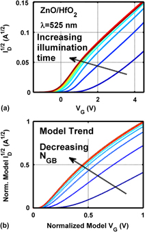
The illumination instabilities of nanocrystalline ZnO thin-film transistors (TFT) with HfO2 gate dielectrics are reported via zero gate bias multiwave length illumination stress method. TFT IDVG curves exhibit a negative threshold voltage shift together with an increase in ID off current and increase in subthreshold slope with increasing photon energy and illumination time. Analysis of transistor characteristics indicates that one component governing negative threshold voltage shifts is a decrease in grain boundary-trapped charge areal density due to illumination. This relationship can be explained by conduction based on thermionic emission over potential barriers formed at the ZnO crystallite boundaries. ID off-state current trends with photon energy in a manner consistent with exponentially decreasing absorption below the conduction band edge.

Type
Reviews
Copyright
Copyright © Materials Research Society 2012

Access options

Get access to the full version of this content by using one of the access options below. (Log in options will check for institutional or personal access. Content may require purchase if you do not have access.)

References

REFERENCES

1.Kwon, J.Y., Lee, K.J., and Kim, K.B.: Review paper: Transparent amorphous oxide semiconductor thin film transistor. Electron. Mater. Lett. 7, 1 (2011).CrossRefGoogle Scholar
2.Conley, J.F.: Instabilities in amorphous oxide semiconductor thin-film transistors. IEEE Trans. Device Mater. Reliab. 10, 4 (2010).CrossRefGoogle Scholar
3.Bayraktaroglu, B., Leedy, K., and Neihard, R.: Nanocrystalline ZnO microwave thin film transistors. Proc. SPIE 7679 (2010).CrossRefGoogle Scholar
4.Siddiqui, J.J., Phillips, J.D., Leedy, K., and Bayraktaroglu, B.: Bias-temperature-stress characteristics of ZnO/HfO2 thin film transistors. IEEE Trans. Electron Devices 49, 14881493 (2012).CrossRefGoogle Scholar
5.Jeong, J.K.: The status and perspectives of metal oxide thin-film transistors for active matrix flexible displays. Semicond. Sci. Technol. 26 (2011).CrossRefGoogle Scholar
6.Shin, J.H., Lee, J.S., Hwang, C.S., Park, S.H.K., Cheong, W.S., Ryu, M., Byun, C.W., Lee, L.I., and Chu, H.Y.: Light effects on the bias stability of transparent ZnO thin film transistors. ETRI 31, 1 (2009).Google Scholar
7.Ji, K.H., Kim, J.I., Mo, Y.G., Jeong, J.H., Yang, S., Hwang, C.S., Park, S.H.K., Ryu, M.K., Lee, S.Y., and Jeong, J.K.: Comparative study on light-induced bias stress instability of IGZO transistors with SiNX and SiO2 gate dielectrics. IEEE Electron Device Lett. 31, 12 (2010).CrossRefGoogle Scholar
8.Yang, S., Cho, D.H., Ryu, M.K., Park, S.H.K., Hwang, C.S., Jang, J., and Jeong, J.K.: Improvement in the photon-induced bias stability of Al-Sn-Zn-In-O thin film transistors by adopting AlOx passivation layer. Appl. Phys. Lett. 96, 213511 (2010).CrossRefGoogle Scholar
9.Kwon, J.Y., Jung, J.S., Son, K.S., Lee, K.H., Park, J.S., Kim, T.S., Park, J.S., Choi, R., Jeong, J.K., Koo, B., and Lee, S.Y.: The impact of gate dielectric materials on the light-induced bias instability in Hf-In-Zn-O thin film transistor. Appl. Phys. Lett. 97, 183503 (2010).CrossRefGoogle Scholar
10.Cross, R.B.M. and De Souza, M.M.: The effect of gate-bias stress and temperature on the performance of ZnO thin-film transistors. IEEE Trans. Device Mater. Reliab. 8, 2 (2008).CrossRefGoogle Scholar
11.Gupta, D., Yoo, S., Lee, C., and Hong, Y.: Electrical-stress-induced threshold voltage instability in solution-processed ZnO thin-film transistors: An experimental and simulation study. IEEE Trans. Electron Devices 58, 7 (2011).CrossRefGoogle Scholar
12.Levinson, J., Shepherd, F.R., Scanlon, P.J., Westwood, W.D., Este, G., and Rider, M.: Condcutivity behavior in polycrystalline semiconductor thin film transistors. J. Appl. Phys. 53, 2 (1982).CrossRefGoogle Scholar