Hostname: page-component-78c5997874-94fs2 Total loading time: 0 Render date: 2024-11-15T21:14:48.832Z Has data issue: false hasContentIssue false

Graphene and monolayer transition-metal dichalcogenides: properties and devices

Published online by Cambridge University Press:  26 January 2016

Olaf M.J. van 't Erve*
Affiliation:
Naval Research Laboratory, Washington, D.C. 20375, USA
Aubrey T. Hanbicki
Affiliation:
Naval Research Laboratory, Washington, D.C. 20375, USA
Adam L. Friedman
Affiliation:
Naval Research Laboratory, Washington, D.C. 20375, USA
Kathleen M. McCreary
Affiliation:
Naval Research Laboratory, Washington, D.C. 20375, USA
Enrique Cobas
Affiliation:
Naval Research Laboratory, Washington, D.C. 20375, USA
Connie H. Li
Affiliation:
Naval Research Laboratory, Washington, D.C. 20375, USA
Jeremy T. Robinson
Affiliation:
Naval Research Laboratory, Washington, D.C. 20375, USA
Berend T. Jonker
Affiliation:
Naval Research Laboratory, Washington, D.C. 20375, USA
*
a)Address all correspondence to this author. e-mail: [email protected]
Get access

Abstract

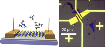
2D materials play a special role in the race to make smaller and smaller devices. Their unique and strong in-plane bonding makes them impervious to diffusion into other layers and provides excellent thickness control. Their van der Waal's bonding with other monolayers or substrates allows for heterostructures unattainable by any other technique. This is reflected by the abundant popularity of research into graphene and other 2D materials. In this review article, we will describe the out-of-plane properties of graphene and functionalized graphene. We will use three specific examples to illustrate how these out-of-plane properties can be used in spintronic devices, in section “Graphene as a Tunnel Barrier” we will describe a magnetic tunnel junction (MTJ) based on graphene. Section “Graphene Based MTJs” will describe the spin injecting properties of a graphene tunnel barrier on silicon. Section “Graphene in Semiconductor Spintronic Devices” describes how you can use functionalized graphene to make a homoepitaxial graphene device. The second part of this article reviews monolayer transition-metal dichalcogenides (TMDs). First, we will show how TMDs are grown and specifically how we can grow large-area TMDs by chemical vapor deposition. Secondly, we will describe the optical properties of several TMDs and compare the results from several authors. Finally, we choose a chemical sensor as a specific example to show how TMDs can be used in a device.

Type
Review
Copyright
Copyright © Materials Research Society 2016 

Access options

Get access to the full version of this content by using one of the access options below. (Log in options will check for institutional or personal access. Content may require purchase if you do not have access.)

References

REFERENCES

Tombros, N., Jozsa, C., Popinciuc, M., Jonkman, H.T., and van Wees, B.J.: Electronic spin transport and spin precession in single graphene layers at room temperature. Nature 448(7153), 571 (2007).CrossRefGoogle ScholarPubMed
Ohishi, M., Shiraishi, M., Nouchi, R., Nozaki, T., Shinjo, T., and Suzuki, Y.: Spin injection into a graphene thin film at room temperature. Jpn. J. Appl. Phys. 46, L605 (2007).Google Scholar
Han, W., Pi, K., McCreary, K.M., Li, Y., Wong, J.J.I., Swartz, A.G., and Kawakami, R.K.: Tunneling spin injection into single layer graphene. Phys. Rev. Lett. 105(16), 167202 (2010).CrossRefGoogle ScholarPubMed
Lee, Y-H., Kim, Y-L., and Lee, J.H.: Vertical conduction behavior through atomic graphene device under transverse electric field. Appl. Phys. Lett. 98, 133112 (2011).Google Scholar
Krishnan, K.S. and Ganguli, N.: Large anisotropy of the electrical conductivity of graphite. Nature 144, 667 (1939).Google Scholar
Chen, S., Brown, L., Levendorf, M., Cai, W., Ju, S-Y., Edgeworth, J., Li, X., Magnuson, C.W., Velamakanni, A., Piner, R.D., Kang, J., Park, J., and Ruoff, R.S.: Oxidation resistance of graphene-coated Cu and Cu/Ni alloy. ACS Nano 5, 1321 (2011).CrossRefGoogle Scholar
Martin, M.B., Dlubak, B., Weatherup, R.S., Piquemal-Banci, M., Yang, H., Blume, R., Schloegl, R., Collin, S., Petroff, F., Hofmann, S., Robertson, J., Anane, A., Fert, A., and Seneor, P.: Protecting nickel with graphene spin-filtering membranes: A single layer is enough. Appl. Phys. Lett. 107(1), 012408 (2015).Google Scholar
Karpan, V.M., Giovanetti, G., Khomyakov, P.A., Talanana, M., Starikov, A.A., Zwierzycki, M., van den Brink, J., Brocks, G., and Kelly, P.J.: Graphite and graphene as perfect spin filters. Phys. Rev. Lett. 99, 176602 (2007).CrossRefGoogle ScholarPubMed
Yazyev, O.V. and Pasquarello, A.: Magnetoresistive junctions based on epitaxial graphene and hexagonal boron nitride. Phys. Rev. B 80, 035408 (2009).Google Scholar
Schmidt, G., Ferrand, D., Molenkamp, L.W., Filip, A.T., and van Wees, B.J.: Fundamental obstacle for electrical spin injection from a ferromagnetic metal into a diffuse semiconductor. Phys. Rev. B 62, R4790 (2000).Google Scholar
Rashba, E.I.: Theory of electrical spin injection: Tunnel contacts as a solution of the conductivity mismatch problem. Phys. Rev. B 62, R16267 (2000).Google Scholar
Fert, A. and Jaffres, H.: Conditions for efficient spin injection from a ferromagnetic metal into a semiconductor. Phys. Rev. B 64, 184420 (2001).CrossRefGoogle Scholar
Awschalom, D.D. and Flatte, M.E.: Challenges for semiconductor spintronics. Nat. Phys. 3, 153 (2007).Google Scholar
Zutic, I., Fabian, J., and Das Sarma, S.: Spintronics: Fundamentals and applications. Rev. Mod. Phys. 76, 323 (2004).CrossRefGoogle Scholar
Sugahara, S. and Nitta, J.: Spin-transistor electronics: An overview and outlook. Proc. IEEE 98, 2124 (2010).CrossRefGoogle Scholar
Dery, H., Dalal, P., Cywinski, L., and Sham, L.J.: Spin-based logic in semiconductors for reconfigurable large-scale circuits. Nature 447, 573576 (2007).CrossRefGoogle ScholarPubMed
Dery, H., Song, Y., Li, P., and Zutic, I.: Silicon spin communication. Appl. Phys. Lett. 99, 082502 (2011).Google Scholar
Tanaka, M. and Sugahara, S.: MOS-based spin devices for reconfigurable logic. IEEE Trans. Electron Devices 54, 961976 (2007).CrossRefGoogle Scholar
Behin-Aein, B., Datta, D., Salahuddin, S., and Datta, S.: Proposal for an all-spin logic device with built-in memory. Nat. Nanotechnol. 5, 266269 (2010).CrossRefGoogle ScholarPubMed
Kawahara, T., Ito, K., Takemura, R., and Ohno, H.: Spin-transfer torque RAM technology: Review and prospect. Microelectron. Reliab. 52, 613 (2012).CrossRefGoogle Scholar
Moodera, J.S., Kinder, L.R., Wong, T.M., and Meservey, R.: Large magnetoresistance at room temperature in ferromagnetic thin film tunnel junctions. Phys. Rev. Lett. 74(16), 3273 (1995).CrossRefGoogle ScholarPubMed
Miyazaki, T. and Tezuka, N.: Giant magnetic tunneling effect in Fe/Al2O3/Fe junction. J. Magn. Magn. Mater. 139, 231 (1995).CrossRefGoogle Scholar
Cobas, E., Friedman, A.L., van 't Erve, O.M.J., Robinson, J.T., and Jonker, B.T.: Graphene as a tunnel barrier: Graphene-based magnetic tunnel junctions. Nano Lett. 12, 3000 (2012).Google Scholar
Cobas, E., Friedman, A.L., van 't Erve, O.M.J., Robinson, J.T., and Jonker, B.T.: Graphene-based magnetic tunnel junctions. IEEE Trans. Magn. 49, 4343 (2013).Google Scholar
van 't Erve, O.M.J., Friedman, A.L., Cobas, E., Li, C.H., Robinson, J.T., and Jonker, B.T.: Low-resistance spin injection into silicon using graphene tunnel barriers. Nat. Nanotechnol. 7(11), 737 (2012).CrossRefGoogle ScholarPubMed
van 't Erve, O.M.J., Friedman, A.L., Cobas, E., Li, C.H., Hanbicki, A.T., McCreary, K.M., Robinson, J.T., and Jonker, B.T.: A graphene solution to conductivity mismatch: Spin injection from ferromagnetic metal/graphene tunnel contacts into silicon. J. Appl. Phys. 113(17), 17C502 (2013).Google Scholar
van 't Erve, O.M.J., Friedman, A.L., Cobas, E., Li, C.H., Robinson, J.T., and Jonker, B.T.: Nonlocal spin valves and nonlocal Hanle using graphene barriers on Silicon. To be published.Google Scholar
van 't Erve, O.M., Friedman, A.L., Li, C.H., Robinson, J.T., Connell, J., Lauhon, L.J., and Jonker, B.T.: Spin transport and Hanle effect in silicon nanowires using graphene tunnel barriers. Nat. Commun. 6, 7541 (2015).Google Scholar
Banerjee, T., van der Wiel, W.G., and Jansen, R.: Spin injection and perpendicular spin transport in graphite nanostructures. Phys. Rev. B 81, 214409 (2010).CrossRefGoogle Scholar
Iqbal, M.Z., Iqbal, M.W., Lee, J.H., Kim, Y.S., Chun, S-H., and Eom, J.: Spin valve effect of NiFe/graphene/NiFe junctions. Nano Res. 6(5), 373 (2013).Google Scholar
Chen, J-J., Meng, J., Zhou, Y-B., Wu, H-C., Bie, Y-Q., Liao, Z-M., and Yu, D-P.: Layer-by-layer assembly of vertically conducting graphene devices. Nat. Commun. 4, 1921 (2013).Google Scholar
Dlubak, B., Seneor, P., Anane, A., Barraud, C., Deranlot, C., Deneuve, D., Servet, B., Mattana, R., Petroff, F., and Fert, A.: Are Al2O3 and MgO tunnel barriers suitable for spin injection in graphene? Appl. Phys. Lett. 97, 092502 (2010).Google Scholar
Mohiuddin, T.M.G., Hill, E., Elias, D., Zhukov, A., Novoselov, K., and Geim, A.: Graphene in multilayers CPP spin valves. IEEE Trans. Magn. 44, 26242627 (2008).Google Scholar
Acik, M. and Chabal, Y.J.: Nature of graphene edges: A review. Jpn. J. Appl. Phys. 50, 070101 (2011).Google Scholar
Li, X., Magnuson, C.W., Venugopal, A., Tromp, R.M., Hannon, J.B., Vogel, E.M., Colombo, L., and Ruoff, R.S.: Large-area graphene single crystals grown by low-pressure chemical vapor deposition of methane on copper. J. Am. Chem. Soc. 133, 2816 (2011).CrossRefGoogle ScholarPubMed
Jonsson-Akerman, B.J., Escudero, R., Leighton, C., Kim, S., Schuller, I.K., and Rabson, D.A.: Reliability of normal-state current–voltage characteristics as an indicator of tunnel-junction barrier quality. Appl. Phys. Lett. 77(12), 1870 (2000).CrossRefGoogle Scholar
Sze, S.M. and Ng, K.K.: Physics of semiconductor devices (John Wiley & Sons Inc., Hoboken, New Jersey, 2007).Google Scholar
Karpan, V.M., Khomyakov, P.A., Starikov, A.A., Giovannetti, G., Zwierzycki, M., Talanana, M., Brocks, G., van den Brink, J., and Kelly, P.J.: Theoretical prediction of perfect spin filtering at interfaces between close-packed surfaces of Ni or Co and graphite or graphene. Phys. Rev. B 78, 195419 (2008).Google Scholar
Butler, W.H., Zhang, X.G., Schulthess, T.C., and MacLaren, J.M.: Spin-dependent tunneling conductance of Fe|MgO|Fe sandwiches. Phys. Rev. B 63, 054416 (2001).CrossRefGoogle Scholar
Mathon, J. and Umerski, A.: Theory of tunneling magnetoresistance of an epitaxial Fe|MgO|Fe(001) junction. Phys. Rev. B 63, 220403 (2001).Google Scholar
Bowen, M., Cros, V., Petroff, F., Fert, A., Martinez Boubeta, C., Costa-Kramer, J.L., Anguita, J.V., Cebollada, A., Briones, F., de Teresa, J.M., Morellon, L., Ibarra, M.R., Guell, F., Peiro, F., and Cornet, A.: Large magnetoresistance in Fe/MgO/Fe(001) epitaxial tunnel junctions on GaAs(001). Appl. Phys. Lett. 79, 1655 (2001).Google Scholar
Parkin, S.S.P., Kaiser, C., Panchula, A., Rice, P.M., Hughes, B., Samant, M., and Yang, S-H.: Giant tunneling magnetoresistance at room temperature with MgO (001) tunnel barriers. Nat. Mater. 3, 862 (2004).CrossRefGoogle Scholar
Yuasa, S., Nagahama, T., Fukushima, A., Suzuki, Y., and Ando, K.: Giant room-temperature magnetoresistance in single-crystal Fe/MgO/Fe magnetic tunnel junctions. Nat. Mater. 3, 868 (2004).Google Scholar
Cobas, E., van 't Erve, O.M.J., Robinson, J., and Jonker, B.: To be published.Google Scholar
Jansen, R.: Silicon spintronics. Nat. Mater. 11(5), 400 (2012).Google Scholar
Monsma, D.J. and Parkin, S.S.P.: Spin polarization of tunneling current from ferromagnet Al2O3 interfaces using copper-doped aluminum superconducting films. Appl. Phys. Lett. 77, 31 (2000).CrossRefGoogle Scholar
Hanbicki, A.T., Jonker, B.T., Itskos, G., Kioseoglou, G., and Petrou, A.: Efficient electrical spin injection from a magnetic metal/tunnel barrier contact into a semiconductor. Applied Physics Letters 80(7), 1240 (2002).Google Scholar
Hanbicki, A.T., van 't Erve, O.M.J., Magno, R., Kioseoglou, G., Li, C.H., Jonker, B.T., Itskos, G., Mallory, R., Yasar, M., and Petrou, A.: Analysis of the transport process providing spin injection through an Fe/AlGaAs Schottky barrier. Appl. Phys. Lett. 82(23), 4092 (2003).Google Scholar
Dash, S.P., Sharma, S., Patel, R.S., de Jong, M.P., and Jansen, R.: Electrical creation of spin polarization in silicon at room temperature. Nature 462(7272), 491 (2009).CrossRefGoogle ScholarPubMed
Jansen, R., Min, B.C., Dash, S.P., Sharma, S., Kioseoglou, G., Hanbicki, A.T., van 't Erve, O.M.J., Thompson, P.E., and Jonker, B.T.: Electrical spin injection into moderately doped silicon enabled by tailored interfaces. Phys. Rev. B 82(24), 241305R (2010).Google Scholar
Li, C.H., van 't Erve, O.M.J., and Jonker, B.T.: Electrical injection and detection of spin accumulation in silicon at 500 K with magnetic metal/silicon dioxide contacts. Nat. Commun. 2, 245 (2011).CrossRefGoogle ScholarPubMed
Gray, N.W. and Tiwari, A.: Room temperature electrical injection and detection of spin polarized carriers in silicon using MgO tunnel barrier. Appl. Phys. Lett. 98(10), 102112 (2011).Google Scholar
Ishikawa, M., Sugiyama, H., Inokuchi, T., Hamaya, K., and Saito, Y.: Effect of the interface resistance of CoFe/MgO contacts on spin accumulation in silicon. Appl. Phys. Lett. 100(25), 252404 (2012).Google Scholar
Ando, Y., Kasahara, K., Yamada, S., Maeda, Y., Masaki, K., Hoshi, Y., Sawano, K., Miyao, M., and Hamaya, K.: Temperature evolution of spin accumulation detected electrically in a nondegenerated silicon channel. Phys. Rev. B 85(3), 035320 (2012).CrossRefGoogle Scholar
Sugiyama, H., Ishikawa, M., Inokuchi, T., Tanamoto, T., Saito, Y., and Tezuka, N.: Large spin-accumulation signal in Si for epitaxial CoFe/highly (100)-textured MgO/Si devices. Solid State Commun. 190, 49 (2014).Google Scholar
Tran, M., Jaffrès, H., Deranlot, C., George, J.M., Fert, A., Miard, A., and Lemaître, A.: Enhancement of the spin accumulation at the interface between a spin-polarized tunnel junction and a semiconductor. Phys. Rev. Lett. 102(3), 036601 (2009).Google Scholar
Jansen, R., Deac, A.M., Saito, H., and Yuasa, S.: Injection and detection of spin in a semiconductor by tunneling via interface states. Phys. Rev. B 85(13), (2012).Google Scholar
Klasges, R., Carbone, C., Eberhardt, W., Pampuch, C., Rader, O., Kachel, T., and Gudat, W.: Formation of a ferromagnetic silicide at the Fe/Si(100) interface. Phys. Rev. B 56, 10801 (1997).Google Scholar
Jansen, R. and Modeera, J.S.: Magnetoresistance in doped magnetic tunnel junctions: Effect of spin scattering and impurity-assisted transport. Phys Rev. B. 61, 9047 (2000).Google Scholar
Zaleski, A., Wrona, J., Czapkiewicz, M., Skowroński, W., Kanak, J., and Stobiecki, T.: The study of conductance in magnetic tunnel junctions with a thin MgO barrier: The effect of Ar pressure on tunnel magnetoresistance and resistance area product. J. Appl. Phys. 111(3), 033903 (2012).CrossRefGoogle Scholar
Chae, J., Jung, S., Woo, S., Baek, H., Ha, J., Song, Y.J., Son, Y-W., Zhitenev, N.B., Stroscio, J.A., and Kuk, Y.: Enhanced carrier transport along edges of graphene devices. Nano Lett. 12(4), 1839 (2012).CrossRefGoogle ScholarPubMed
Simmons, J.G.: Generalized Formula for the electric tunnel effect between similar electrodes separated by a thin insulating film. J. Appl. Phys. 34(6), 1793 (1963).Google Scholar
Brinkman, W.F., Dynes, R.C., and Rowell, J.M.: Tunneling conductance of asymmetrical barriers. J. Appl. Phys. 41, 1915 (1970).Google Scholar
Meservey, R. and Tedrow, P.M.: Spin-polarized electron tunneling. Phys. Rep. 238, 173243 (1994).Google Scholar
Sasaki, T., Oikawa, T., Suzuki, T., Shiraishi, M., Suzuki, Y., and Noguchi, K.: Temperature dependence of spin diffusion length in silicon by Hanle-type spin precession. Appl. Phys. Lett. 96(12), 122101 (2010).Google Scholar
Suzuki, T., Sasaki, T., Oikawa, T., Shiraishi, M., Suzuki, Y., and Noguchi, K.: Room-temperature electron spin transport in a highly doped Si channel. Appl. Phys. Express 4(2), 023003 (2011).Google Scholar
Shiraishi, M., Honda, Y., Shikoh, E., Suzuki, Y., Shinjo, T., Sasaki, T., Oikawa, T., Noguchi, K., and Suzuki, T.: Spin transport properties in silicon in a nonlocal geometry. Phys. Rev. B 83(24), 241204R (2011).Google Scholar
Min, B-C., Motohashi, K., Lodder, C., and Jansen, R.: Tunable spin-tunnel contacts to silicon using low-work-function ferromagnets. Nat. Mater. 5(10), 817 (2006).CrossRefGoogle ScholarPubMed
Mohney, S.E., Wang, Y., Cabassi, M.A., Lew, K.K., Dey, S., Redwing, J.M., and Mayer, T.S.: Measuring the specific contact resistance of contacts to semiconductor nanowires. Solid-State Electron. 49(2), 227 (2005).Google Scholar
Leonard, F. and Talin, A.A.: Electrical contacts to one- and two-dimension nanomaterials. Nat. Nanotechnol. 6, 773783 (2011).Google Scholar
Johnson, M. and Silsbee, R.H.: Interfacial charge-spin coupling: Injection and detection of spin magnetization in metals. Phys. Rev. Lett. 55, 17901793 (1985).Google Scholar
Jedema, F., Nijboer, M., Filip, A., and van Wees, B.: Spin injection and spin accumulation in all-metal mesoscopic spin valves. Phys. Rev. B 67, 085319 (2003).Google Scholar
Lou, X., Adelmann, C., Furis, M., Crooker, S., Palmstrøm, C., and Crowell, P.: Electrical detection of spin accumulation at a ferromagnet-semiconductor interface. Phys. Rev. Lett. 96(17), 176603 (2006).Google Scholar
Cui, Y., Lauhon, L.J., Gudiksen, M.S., Wang, J.F., and Lieber, C.M.: Diameter-controlled synthesis of single-crystal silicon nanowires. Appl. Phys. Lett. 78, 22142216 (2001).Google Scholar
Jin, J.E., Lee, J.H., Hwang, D.H., Kim, D.W., Kim, M.J., Son, K.S., Whang, D., and Hwang, S.W.: Graphene arch gate SiO2 shell silicon nanowire core field effect transistors. Appl. Phys. Lett. 99(21), 212102 (2011).Google Scholar
Zhang, S., Dayeh, S.A., Li, Y., Crooker, S.A., Smith, D.L., and Picraux, S.T.: Electrical spin injection and detection in silicon nanowires through oxide tunnel barriers. Nano Lett. 13, 430435 (2013).Google Scholar
Lou, X., Adelmann, C., Crooker, S.A., Garlid, E.S., Zhang, J., Reddy, K.S.M., Flexner, S.D., Palmstrøm, C.J., and Crowell, P.A.: Electrical detection of spin transport in lateral ferromagnet–semiconductor devices. Nat. Phys. 3(3), 197 (2007).Google Scholar
Han, W., Kawakami, R.K., Gmitra, M., and Fabian, J.: Graphene spintronics. Nat. Nanotechnol. 9, 794 (2014).Google Scholar
Friedman, A.L., van 't Erve, O.M.J., Li, C., Robinson, J.T., and Jonker, B.T.: Homoepitaxial tunnel barriers with functionalized graphene on graphene for charge and spin transport. Nat. Commun. 5, 3161 (2014).CrossRefGoogle ScholarPubMed
Friedman, A.L., van't Erve, O.M.J., Robinson, J.T., Whitener, K.E. Jr., and Jonker, B.T.: Hydrogenated graphene as a homoepitaxial tunnel barrier for charge and spin transport in graphene. ACS Nano 9(7), 67476755 (2015).Google Scholar
Popinciuc, M., Jozsa, C., Zomer, P.J., Tombros, N., Veligura, A., Jonkman, H.T., and van Wees, B.J.: Electronic spin transport in graphene field-effect transistors. Phys. Rev. B. 80(21), 214427 (2009).Google Scholar
Avsar, A., Yang, T-Y., Bae, S., Balakrishnan, J., Volmer, F., Jaiswal, M., Yi, Z., Ali, S.R., Güntherodt, G., Hong, B.H., Beschoten, B., and Özyilmaz, B.: Toward wafer scale fabrication of graphene based spin valve devices. Nano Lett. 11(6), 2363 (2011).CrossRefGoogle ScholarPubMed
Guimaraes, M.H., Veligura, A., Zomer, P.J., Maassen, T., Vera-Marun, I.J., Tombros, N., and van Wees, B.J.: Spin transport in high quality suspended graphene devices. Nano Lett. 12, 3512 (2012).Google Scholar
Sosenko, E., Wei, H., and Aji, V.: Effect of contacts on spin lifetime measurements in graphene. Phys. Rev. B 89, 245436 (2014).Google Scholar
Pesin, D. and MacDonald, A.H.: Spintronics and pseudospintronics in graphene and topological insulators. Nat. Mater. 11, 409 (2012).Google Scholar
Friedman, A.L., Robinson, J.T., Keith Perkins, F., and Campbell, P.M.: Extraordinary magnetoresistance in CVD grown graphene devices. Appl. Phys. Lett. 99, 022108 (2011).CrossRefGoogle Scholar
Friedman, A.L., Tedesco, J.L., Campbell, P.M., Culbertson, J.C., Aifer, E., Keith Perkins, F., Myers-Ward, R.L., Hite, J.K., Jernigan, G.G., Eddy, C.R. Jr., and Kurt Gaskill, D.: Quantum linear magnetoresistance in multilayer epitaxial graphene. Nano Lett. 10, 3962 (2010).Google Scholar
Nyakitit, L.O., Myers-Ward, R.L., Wheeler, V.D., Imhoff, E.A., Bezares, F.J., Caldwell, J.D., Friedman, A.L., Matis, B.R., Baldwin, J.W., Campbell, P.M., Culbertson, J.C., Eddy, C.R. Jr., Jernigan, G.G., Chun, H., and Kurt Gaskill, D.: Bilayer graphene grown on 4H-SiC (0001) step-free mesas. Nano Lett. 12(4), 17491756 (2012).Google Scholar
Cress, C.D., Champlain, J.G., Esqueda, I.S., Robinson, J.T., Friedman, A.L., and McMorrow, J.J.: Total ionizing dose induced charge carrier scattering in graphene devices. IEEE Trans. Nucl. Sci. 59(6), 30453053 (2012).Google Scholar
Kretinin, A.V., Cao, Y., Tu, J.S., Yu, G.L., Jalil, R., Novoselov, K.S., Haigh, S.J., Gholinia, A., Mishchenko, A., Lozada, M., Georgiou, T., Woods, C.R., Withers, F., Blake, P., Eda, G., Wirsig, A., Hucho, C., Watanabe, K., Tanigushi, T., Geim, A.K., and Gorbachev, R.V.: Electronic properties of graphene encapsulated with different two-dimensional atomic crystals. Nano Lett. 14(6), 3270 (2014).Google Scholar
Neumann, I., Costache, M.V., Bridoux, G., Sierra, J.F., and Valenzuela, S.O.: Enhanced spin accumulation at room temperature in graphene spin valves with amorphous carbon interfacial layers. Appl. Phys. Lett. 103, 112401 (2013).Google Scholar
Yamaguchi, T., Inoue, Y., Masubuchi, S., Morikawa, S., Onuki, M., Watanabe, K., Taniguchi, T., Moriya, R., and Machida, T.: Electrical spin injection into graphene through monolayer hexagonal boron nitride. Appl. Phys. Express 6, 073001 (2013).CrossRefGoogle Scholar
Chae, D-H., Zhang, D., Huang, X., and von Klitzing, K.: Electronic transport in two stacked graphene monolayers. Nano Lett. 12, 3905 (2012).Google Scholar
Jernigan, G.G., Anderson, T.J., Robinson, J.T., Caldwell, J.D., Culbertson, J.C., Myers-Ward, R., Davidson, A.L., Ancona, M.G., Wheeler, V.D., Nyakiti, L.O., Friedman, A.L., Campbell, P.M., and Kurt Gaskill, D.: Bilayer graphene by bonding CVD graphene to epitaxial graphene. J. Vac. Sci. Technol., B 30, 03D110 (2012).Google Scholar
Robinson, J.T., Schmucker, S.W., Diaconescu, B., Long, J.P., Culbertson, J.C., Ohta, T., Friedman, A.L., and Beechem, T.: Electronic hybridization of stacked graphene films. ACS Nano 7(1), 637644 (2013).Google Scholar
Robinson, J.T., Burgess, J.S., Junkermeier, C.E., Badescu, S.C., Reinecke, T.L., Perkins, F.K., Zalalutdinov, M.K., Baldwin, J.W., Culbertson, J.C., Sheehan, P.E., and Snow, E.S.: Properties of fluorinated graphene films. Nano Lett. 10(8), 30013005 (2010).Google Scholar
Stine, R., Lee, W.K., Whitener, K.E. Jr., Robinson, J.T., and Sheehan, P.E.: Chemical stability of graphene fluoride produced by exposure to XeF2 . ACS Nano 13(9), 43114316 (2013).Google Scholar
Matis, B.R., Bulat, F.A., Friedman, A.L., Houston, B.H., and Baldwin, J.W.: Giant negative magnetoresistance and a transition from strong to weak localization in hydrogenated graphene. Phys. Rev. B 85, 105437 (2012).Google Scholar
Matis, B.R., Burgass, J.S., Bulat, F.A., Friedman, A.L., Houston, B.H., and Baldwin, J.W.: Surface doping and bandgap tunability in hydrogenated graphene. ACS Nano 6(1), 1722 (2012).Google Scholar
Matis, B.R., Bulat, F.A., Friedman, A.L., Houston, B.H., and Baldwin, J.W.: Chemically functionalized graphene for bipolar electronics. Appl. Phys. Lett. 102, 103114 (2013).Google Scholar
Miao, G., Munzengerg, M., and Moodera, J.: Tunneling path toward spintronics. Rep. Prog. Phys. 74, 036501 (2011).CrossRefGoogle Scholar
Wang, M. and Li, C.M.: Investigation of doping effects on magnetic properties of the hydrogenated and fluorinated graphene structures by extra charge mimic. Phys. Chem. Chem. Phys. 15, 3786 (2013).Google Scholar
Dev, P. and Reinecke, T.L.: Substrate effects: Disappearance of adsorbate-induced magnetism in graphene. Phys. Rev. B 89, 035404 (2014).Google Scholar
Lee, W.K., Whitener, K.E. Jr., Robinson, J.T., and Sheehan, P.E.: Patterning magnetic regions in hydrogenated graphene via e-beam irradiation. Adv. Mater. 27, 1774 (2015).Google Scholar
Friedman, A.L., Chun, H., Jung, Y.J., Glaser, E.R., Heiman, D., and Menon, L.: Possible room-temperature ferromagnetism in hydrogenated carbon nanotubes. Phys. Rev. B 81, 115461 (2010).Google Scholar
Volmer, F., Drogeler, M., Maynicke, E., von den Driesch, N., Boschen, M.L., Guntherodt, G., and Beschoten, B.: Role of MgO barriers for spin and charge transport in Co/MgO/graphene nonlocal spin-valve devices. Phys. Rev. B 88, 161405(R) (2013).Google Scholar
Jariwala, D., Sangwan, V.K., Lauhon, L.J., Marks, T.J., and Hersam, M.C.: Emerging device applications for semiconducting two-dimensional transition metal dichalcogenides. ACS Nano 8, 11021120 (2014).Google Scholar
Das, S., Robinson, J.A., Dubey, M., Terrones, H., and Terrones, M.: Beyond graphene: Progress in novel two-dimensional materials and van der Waals solids. Annu. Rev. Mater. Res. 45, 127 (2015).Google Scholar
Novoselov, K.S., Jiang, D., Schedin, F., Booth, T.J., Khotkevich, V.V., Morozov, S.V., and Geim, A.K.: Two-dimensional atomic crystals. Proc. Natl. Acad. Sci. U. S. A. 102, 10451 (2005).Google Scholar
Wang, Q.H., Kalantar-Zadeh, K., Kis, A., Coleman, J.N., and Strano, M.S.: Electronics and optoelectronics of two-dimensional transition metal dichalcogenides. Nat. Nanotechnol. 7(11), 699 (2012).Google Scholar
Najmaei, S., Liu, Z., Zhou, W., Zou, X., Shi, G., Lei, S., Yakobson, B.I., Idrobo, J-C., Ajayan, P.M., and Lou, J.: Vapour phase growth and grain boundary structure of molybdenum disulphide atomic layers. Nat. Mater. 12, 754 (2013).Google Scholar
Novoselov, K.S., Geim, A.K., Morozov, S.V., Jiang, D., Katsnelson, M.I., Grigorieva, I.V., Dubonos, S.V., and Firsov, A.A.: Two-dimensional gas of massless Dirac fermions in graphene. Nature 438, 197 (2005).Google Scholar
Iqbal, M.W., Iqbal, M.Z., Khan, M.F., Shehzad, M.A., Seo, Y., Park, J.H., Hwang, C., and Eom, J.: High-mobility and air-stable single-layer WS2 field-effect transistors sandwiched between chemical vapor deposition-grown hexagonal BN films. Sci. Rep. 5, 10699 (2015).Google Scholar
Kaasbjerg, K., Thygesen, K.S., and Jacobsen, K.W.: Phonon-limited mobility in n-type single-layer MoS2 from first principles. Phys. Rev. B 85, 115317 (2012).Google Scholar
Mak, K.F., Lee, C., Hone, J., Shan, J., and Heinz, T.F.: Atomically thin MoS2: A new direct-gap semiconductor. Phys. Rev. Lett. 105, 136805 (2010).Google Scholar
Perkins, F.K., Friedman, A.L., Cobas, E., Campbell, P.M., Jernigan, G.G., and Jonker, B.T.: Chemical vapor sensing with monolayer MoS2 . Nano Lett. 13, 668673 (2013).Google Scholar
Mak, K.F., He, K., Shan, J., and Heinz, T.F.: Control of valley polarization in monolayer MoS2 by optical helicity. Nat. Nanotechnol. 7, 494 (2012).Google Scholar
Kioseoglou, G., Hanbicki, A.T., Currie, M., Friedman, A.L., Gunlycke, D., and Jonker, B.T.: Valley polarization and intervalley scattering in monolayer MoS2 . Appl. Phys. Lett. 101, 221907 (2012).CrossRefGoogle Scholar
Yang, L., Sinitsyn, N.A., Chen, W., Yuan, J., Zhang, J., Lou, J., and Crooker, S.A.: Long-lived nanosecond spin relaxation and spin coherence of electrons in monolayer MoS2 and WS2 . Nat. Phys. 11(10), 830 (2015).Google Scholar
Splendiani, A., Sun, L., Zhang, Y., Li, T., Kim, J., Chim, C-Y., Galli, G., and Wang, F.: Emerging photoluminescence in monolayer MoS2 . Nano Lett. 10, 12711275 (2010).Google Scholar
Radisavljevic, B., Radenovic, A., Brivio, J., Giacometti, V., and Kis, A.: Single-layer MoS2 transistors. Nat. Nanotechnol. 6, 147150 (2011).Google Scholar
Song, J-G., Park, J., Lee, W., Choi, T., Jung, H., Lee, C.W., Hwang, S-H., Myoung, J.M., Jung, J-H., Kim, S-H., Lansalot-Matras, C., and Kim, H.: Layer-controlled, wafer-scale, and conformal synthesis of tungsten disulfide nanosheets using atomic layer deposition. ACS Nano 7, 11333 (2013).Google Scholar
Zhang, Y., Chang, T-R., Zhou, B., Cui, Y-T., Yan, H., Liu, Z., Schmitt, F., Lee, J., Moore, R., Chen, Y., Lin, H., Jeng, H-T., Mo, S-K., Hussain, Z., Bansil, A., and Shen, Z-X.: Direct observation of the transition from indirect to direct bandgap in atomically thin epitaxial MoSe2 . Nat. Nanotechnol. 9, 111 (2014).Google Scholar
Zhan, Y., Liu, Z., Najmaei, S., Ajayan, P.M., and Lou, J.: Large-area vapor-phase growth and characterization of MoS2 atomic layers on a SiO2 substrate. Small 8, 966971 (2012).Google Scholar
van der Zande, A.M., Huang, P.Y., Chenet, D.A., Berkelbach, T.C., You, Y., Lee, G-H., Heinz, T.F., Reichman, D.R., Muller, D.A., and Hone, J.C.: Grains and grain boundaries in highly crystalline monolayer molybdenum disulphide. Nat. Mater. 12, 554561 (2013).Google Scholar
Shi, Y., Zhou, W., Lu, A-Y., Fang, W., Lee, Y-H., Hsu, A.L., Kim, S.M., Kim, K.K., Yang, H.Y., Li, L-J., Idrobo, J-C., and Kong, J.: van der Waals epitaxy of MoS2 layers using graphene as growth templates. Nano Lett. 12, 27842791 (2012).Google Scholar
Liu, K-K., Zhang, W., Lee, Y-H., Lin, Y-C., Chang, M-T., Su, C-Y., Chang, C-S., Li, H., Shi, Y., Zhang, H., Lai, C-S., and Li, L-J.: Growth of large-area and highly crystalline MoS2 thin layers on insulating substrates. Nano Lett. 12, 15381544 (2012).Google Scholar
Yu, Y., Li, C., Liu, Y., Su, L., Zhang, Y., and Cao, L.: Controlled scalable synthesis of uniform, high-quality monolayer and few-layer MoS2 films. Sci. Rep. 3, 1866 (2013).Google Scholar
McCreary, K.M., Hanbicki, A.T., Robinson, J.T., Cobas, E., Culbertson, J.C., Friedman, A.L., Jernigan, G.G., and Jonker, B.T.: Large-area synthesis of continuous and uniform MoS2 monolayer films on graphene. Adv. Funct. Mater. 24, 64496454 (2014).Google Scholar
Kang, K., Xie, S., Huang, L., Han, Y., Huang, P.Y., Mak, K.F., Kim, C-J., Muller, D., and Park, J.: High-mobility three-atom-thick semiconducting films with wafer-scale homogeneity. Nature 520, 656660 (2015).Google Scholar
Eichfeld, S.M., Hossain, L., Lin, Y-C., Piasecki, A.F., Kupp, B., Birdwell, A.G., Burke, R.A., Lu, N., Peng, X., Li, J., Azcatl, A., McDonnell, S., Wallace, R.M., Kim, M.J., Mayer, T.S., Redwing, J.M., and Robinson, J.A.: Highly scalable, atomically thin WSe2 grown via metal–organic chemical vapor deposition. ACS Nano 9, 20802087 (2015).Google Scholar
Shaw, J., Zhou, H., Chen, Y., Weiss, N., Liu, Y., Huang, Y., and Duan, X.: Chemical vapor deposition growth of monolayer MoSe2 nanosheets. Nano Res. 7, 1 (2014).Google Scholar
Wang, X., Gong, Y., Shi, G., Chow, W.L., Keyshar, K., Ye, G., Vajtai, R., Lou, J., Liu, Z., Ringe, E., Tay, B.K., and Ajayan, P.M.: Chemical vapor deposition growth of crystalline monolayer MoSe2 . ACS Nano 8, 5125 (2014).Google Scholar
Lee, Y-H., Yu, L., Wang, H., Fang, W., Ling, X., Shi, Y., Lin, C-T., Huang, J-K., Chang, M-T., Chang, C-S., Dresselhaus, M., Palacios, T., Li, L-J., and Kong, J.: Synthesis and transfer of single-layer transition metal disulfides on diverse surfaces. Nano Lett. 13, 1852 (2013).Google Scholar
McCreary, K., Hanbicki, A., Gernigan, G., Culbertson, E., and Jonker, B.: Synthesis of large-area WS2 monolayers with exceptional photoluminescence. Sci. Rep. Recent accept.Google Scholar
Huang, J-K., Pu, J., Hsu, C-L., Chiu, M-H., Juang, Z-Y., Chang, Y-H., Chang, W-H., Iwasa, Y., Takenobu, T., and Li, L-J.: Large-area synthesis of highly crystalline WSe2 monolayers and device applications. ACS Nano 8, 923 (2013).Google Scholar
Liu, B., Fathi, M., Chen, L., Abbas, A., Ma, Y., and Zhou, C.: Chemical vapor deposition growth of monolayer WSe2 with tunable device characteristics and growth mechanism study. ACS Nano 9, 6119 (2015).Google Scholar
Lin, Y-C., Ghosh, R.K., Addou, R., Lu, N., Eichfeld, S.M., Zhu, H., Li, M-Y., Peng, X., Kim, M.J., Li, L-J., Wallace, R.M., Datta, S., and Robinson, J.A.: Atomically thin resonant tunnel diodes built from synthetic van der Waals heterostructures. Nat. Commun. 6, 7311 (2015).Google Scholar
Liu, H., Jiao, L., Yang, F., Cai, Y., Wu, X., Ho, W., Gao, C., Jia, J., Wang, N., Fan, H., Yao, W., and Xie, M.: Dense network of one-dimensional midgap metallic modes in monolayer MoSe2 and their spatial undulations. Phys. Rev. Lett. 113, 066105 (2014).CrossRefGoogle ScholarPubMed
Ugeda, M.M., Bradley, A.J., Shi, S-F., da Jornada, F.H., Zhang, Y., Qiu, D.Y., Ruan, W., Mo, S-K., Hussain, Z., Shen, Z-X., Wang, F., Louie, S.G., and Crommie, M.F.: Giant bandgap renormalization and excitonic effects in a monolayer transition metal dichalcogenide semiconductor. Nat. Mater. 13, 1091 (2014).Google Scholar
Liu, H.J., Jiao, L., Xie, L., Yang, F., and Chen, J.L.: Molecular-beam epitaxy of monolayer and bilayer WSe2: A scanning tunneling microscopy/spectroscopy study and deduction of exciton binding energy. 2D Mater. 2, 034004 (2015).Google Scholar
Pu, J., Yomogida, Y., Liu, K-K., Li, L-J., Iwasa, Y., and Takenobu, T.: Highly flexible MoS2 thin-film transistors with ion gel dielectrics. Nano. Lett. 12, 4013 (2012).Google Scholar
Kong, D., Wang, H., Cha, J.J., Pasta, M., Koski, K.J., Yao, J., and Cui, Y.: Synthesis of MoS2 and MoSe2 films with vertically aligned layers. Nano Lett. 13, 1341 (2013).Google Scholar
Lin, Y-C., Zhang, W., Huang, J-K., Liu, K-K., Lee, Y-H., Liang, C-T., Chu, C-W., and Li, L-J.: Wafer-scale MoS2 thin layers prepared by MoO3 sulfurization. Nanoscale 4, 6637 (2012).Google Scholar
Lee, Y., Lee, J., Bark, H., Oh, I-K., Ryu, G.H., Lee, Z., Kim, H., Cho, J.H., Ahn, J-H., and Lee, C.: Synthesis of wafer-scale uniform molybdenum disulfide films with control over the layer number using a gas phase sulfur precursor. Nanoscale 6, 2821 (2014).Google Scholar
Elías, A.L., Perea-López, N., Castro-Beltrán, A., Berkdemir, A., Lv, R., Feng, S., Long, A.D., Hayashi, T., Kim, Y.A., Endo, M., Gutiérrez, H.R., Pradhan, N.R., Balicas, L., Mallouk, T.E., López-Urías, F., Terrones, H., and Terrones, M.: Controlled synthesis and transfer of large-area WS2 sheets: From single layer to few layers. ACS Nano 7, 5235 (2013).Google Scholar
Gutiérrez, H.R., Perea-López, N., Elías, A.L., Berkdemir, A., Wang, B., Lv, R., López-Urías, F., Crespi, V.H., Terrones, H., and Terrones, M.: Extraordinary room-temperature photoluminescence in triangular WS2 monolayers. Nano Lett. 13, 3447 (2013).Google Scholar
Lin, Y-C., Lu, N., Perea-Lopez, N., Li, J., Lin, Z., Peng, X., Lee, C.H., Sun, C., Calderin, L., Browning, P.N., Bresnehan, M.S., Kim, M.J., Mayer, T.S., Terrones, M., and Robinson, J.A.: Direct synthesis of van der Waals solids. ACS Nano 8, 3715 (2014).Google Scholar
Shi, Y., Li, H., and Li, L-J.: Recent advances in controlled synthesis of two-dimensional transition metal dichalcogenides via vapour deposition techniques. Chem. Soc. Rev. 44, 2744 (2015).Google Scholar
Bosi, M.: Growth and synthesis of mono and few-layers transition metal dichalcogenides by vapour techniques: A review. RSC Adv. 5, 75500 (2015).Google Scholar
Lv, R., Terrones, H., Elías, A.L., Perea-López, N., Gutiérrez, H.R., Cruz-Silva, E., Rajukumar, L.P., Dresselhaus, M.S., and Terrones, M.: Two-dimensional transition metal dichalcogenides: Clusters, ribbons, sheets and more. Nano Today 44, 26152628 (2015).Google Scholar
Ling, X., Lee, Y-H., Lin, Y., Fang, W., Yu, L., Dresselhaus, M.S., and Kong, J.: Role of the seeding promoter in MoS2 growth by chemical vapor deposition. Nano Lett. 14, 464472 (2014).Google Scholar
Lee, Y-H., Zhang, X-Q., Zhang, W., Chang, M-T., Lin, C-T., Chang, K-D., Yu, Y-C., Wang, J.T-W., Chang, C-S., Li, L-J., and Lin, T-W.: Synthesis of large-area MoS2 atomic layers with chemical vapor deposition. Adv. Mater. 24, 23202325 (2012).Google Scholar
Tonndorf, P., Schmidt, R., Böttger, P., Zhang, X., Börner, J., Liebig, A., Albrecht, M., Kloc, C., Gordan, O., Zahn, D.R.T., Michaelis de Vasconcellos, S., and Bratschitsch, R.: Photoluminescence emission and Raman response of monolayer MoS2, MoSe2, and WSe2 . Opt. Express 21, 49084916 (2013).Google Scholar
Chakraborty, B., Bera, A., Muthu, D.V.S., Bhowmick, S., Waghmare, U.V., and Sood, A.K.: Symmetry-dependent phonon renormalization in monolayer MoS2 transistor. Phys. Rev. B 85, 161403 (2012).Google Scholar
Castellanos-Gomez, A., Roldán, R., Cappelluti, E., Buscema, M., Guinea, F., van der Zant, H.S.J., and Steele, G.A.: Local strain engineering in atomically thin MoS2 . Nano Lett. 13, 53615366 (2013).Google Scholar
Buscema, M., Steele, G., Zant, H.J., and Castellanos-Gomez, A.: The effect of the substrate on the Raman and photoluminescence emission of single-layer MoS2 . Nano Res. 7, 111 (2014).Google Scholar
Wang, Y., Cong, C., Yang, W., Shang, J., Peimyoo, N., Chen, Y., Kang, J., Wang, J., Huang, W., and Yu, T.: Strain-induced direct–indirect bandgap transition and phonon modulation in monolayer WS2 . Nano Res. 8, 25622572 (2015).Google Scholar
Zhu, Z.Y., Cheng, Y.C., and Schwingenschlögl, U.: Giant spin-orbit-induced spin splitting in two-dimensional transition-metal dichalcogenide semiconductors. Phys. Rev. B 84, 153402 (2011).Google Scholar
McDonnell, S., Addou, R., Buie, C., Wallace, R.M., and Hinkle, C.L.: Defect-dominated doping and contact resistance in MoS2 . ACS Nano 8, 28802888 (2014).Google Scholar
Addou, R., McDonnell, S., Barrera, D., Guo, Z., Azcatl, A., Wang, J., Zhu, H., Hinkle, C.L., Quevedo-Lopez, M., Alshareef, H.N., Colombo, L., Hsu, J.W.P., and Wallace, R.M.: Impurities and electronic property variations of natural MoS2 crystal surfaces. ACS Nano 9, 91249133 (2015).Google Scholar
Li, M-Y., Shi, Y., Cheng, C-C., Lu, L-S., Lin, Y-C., Tang, H-L., Tsai, M-L., Chu, C-W., Wei, K-H., He, J-H., Chang, W-H., Suenaga, K., and Li, L-J.: Epitaxial growth of a monolayer WSe2-MoS2 lateral p-n junction with an atomically sharp interface. Science 349, 524528 (2015).Google Scholar
Gong, Y., Lin, J., Wang, X., Shi, G., Lei, S., Lin, Z., Zou, X., Ye, G., Vajtai, R., Yakobson, B.I., Terrones, H., Terrones, M., Tay, B.K., Lou, J., Pantelides, S.T., Liu, Z., Zhou, W., and Ajayan, P.M.: Vertical and in-plane heterostructures from WS2/MoS2 monolayers. Nat. Mater. 13, 11351142 (2014).Google Scholar
Geim, A.K. and Grigorieva, I.V.: Van der Waals heterostructures. Nature 499, 419425 (2013).Google Scholar
Yoon, Y., Ganapathi, K., and Salahuddin, S.: How good can monolayer MoS2 transistors Be? Nano Lett. 11, 37683773 (2011).Google Scholar
Alam, K. and Lake, R.K.: Monolayer MoS2 transistors beyond the technology road map IEEE Trans. Electron Devices 59, 32503254 (2012).Google Scholar
Feng, J., Qian, X., Huang, C-W., and Li, J.: Strain-engineered artificial atom as a broad-spectrum solar energy funnel. Nat. Photonics 6, 866872 (2012).Google Scholar
Bernardi, M., Palummo, M., and Grossman, J.C.: Extraordinary sunlight absorption and one nanometer thick photovoltaics using two-dimensional monolayer materials. Nano Lett. 13, 36643670 (2013).Google Scholar
Liu, B., Chen, L., Liu, G., Abbas, A.N., Fathi, M., and Zhou, C.: High-performance chemical sensing using Schottky-contacted chemical vapor deposition grown monolayer MoS2 transistors. ACS Nano 8, 53045314 (2014).Google Scholar
Xiao, D., Liu, G-B., Feng, W., Xu, X., and Yao, W.: Coupled spin and valley physics in monolayers of MoS2 and other group-VI dichalcogenides. Phys. Rev. Lett. 108, 196802 (2012).Google Scholar
Cao, T., Wang, G., Han, W., Ye, H., Zhu, C., Shi, J., Niu, Q., Tan, P., Wang, E., Liu, B., and Feng, J.: Valley-selective circular dichroism of monolayer molybdenum disulphide. Nat. Commun. 3, 887 (2012).Google Scholar
Mak, K.F., McGill, K.L., Park, J., and McEuen, P.L.: The valley Hall effect in MoS2 transistors. Science 344, 14891492 (2014).Google Scholar
Qiu, D.Y., da Jornada, F.H., and Louie, S.G.: Optical spectrum of MoS2: Many-body effects and diversity of exciton states. Phys. Rev. Lett. 111, 216805 (2013).Google Scholar
Hanbicki, A.T., Currie, M., Kioseoglou, G., Friedman, A.L., and Jonker, B.T.: Measurement of high exciton binding energy in the monolayer transition-metal dichalcogenides WS2 and WSe2 . Solid State Commun. 203, 1620 (2015).Google Scholar
Ramasubramaniam, A.: Large excitonic effects in monolayers of molybdenum and tungsten dichalcogenides. Phys. Rev. B 86, 115409 (2012).Google Scholar
He, K., Kumar, N., Zhao, L., Wang, Z., Mak, K.F., Zhao, H., and Shan, J.: Tightly bound excitons in monolayer WSe2 . Phys. Rev. Lett. 113, 026803 (2014).Google Scholar
Chernikov, A., Berkelbach, T.C., Hill, H.M., Rigosi, A., Li, Y., Aslan, O.B., Reichman, D.R., Hybertsen, M.S., and Heinz, T.F.: Exciton binding energy and nonhydrogenic rydberg series in monolayer WS2 . Phys. Rev. Lett. 113, 076802 (2014).Google Scholar
Mak, K.F., He, K., Lee, C., Lee, G.H., Hone, J., Heinz, T.F., and Shan, J.: Tightly bound trions in monolayer MoS2 . Nat. Mater. 12, 207211 (2012).Google Scholar
Ross, J.S., Wu, S., Yu, H., Ghimire, N.J., Jones, A.M., Aivazian, G., Yan, J., Mandrus, D.G., Xiao, D., Yao, W., and Xu, X.: Electrical control of neutral and charged excitons in a monolayer semiconductor. Nat. Commun. 4, 1474 (2013).Google Scholar
Sallen, G., Bouet, L., Marie, X., Wang, G., Zhu, C.R., Han, W.P., Lu, Y., Tan, P.H., Amand, T., Liu, B.L., and Urbaszek, B.: Robust optical emission polarization in MoS2 monolayers through selective valley excitation. Phys. Rev. B 86, 081301 (2012).Google Scholar
Zeng, H., Dai, J., Yao, W., Xiao, D., and Cui, X.: Valley polarization in MoS2 monolayers by optical pumping. Nat. Nanotechnol. 7, 490493 (2012).Google Scholar
Blake, P., Hill, E.W., Castro Neto, A.H., Novoselov, K.S., Jiang, D., Yang, R., Booth, T.J., and Geim, A.K.: Making graphene visible. Appl. Phys. Lett. 91, 063124 (2007).CrossRefGoogle Scholar
Benameur, M.M., Radisavljevic, B., Héron, J.S., Sahoo, S., Berger, H., and Kis, A.: Visibility of dichalcogenide nanolayers. Nanotechnology 22, 125706 (2011).CrossRefGoogle ScholarPubMed
Lee, C., Yan, H., Brus, L.E., Heinz, T.F., Hone, J., and Ryu, S.: Anomalous lattice vibrations of single- and few-layer MoS2 . ACS Nano 4, 26952700 (2010).Google Scholar
Molina-Sánchez, A. and Wirtz, L.: Phonons in single-layer and few-layer MoS2 and WS2 . Phys. Rev. B 84, 155413 (2011).Google Scholar
Berkdemir, A., Gutiérrez, H.R., Botello-Méndez, A.R., Perea-López, N., Elías, A.L., Chia, C-I., Wang, B., Crespi, V.H., López-Urías, F., Charlier, J-C., Terrones, H., and Terrones, M.: Identification of individual and few layers of WS2 using Raman spectroscopy. Sci. Rep. 3, 1755 (2013).Google Scholar
Sahin, H., Tongay, S., Horzum, S., Fan, W., Zhou, J., Li, J., Wu, J., and Peeters, F.M.: Anomalous Raman spectra and thickness-dependent electronic properties of WSe2 . Phys. Rev. B 87, 165409 (2013).Google Scholar
Terrones, H., Corro, E.D., Feng, S., Poumirol, J.M., Rhodes, D., Smirnov, D., Pradhan, N.R., Lin, Z., Nguyen, M.A.T., Elías, A.L., Mallouk, T.E., Balicas, L., Pimenta, M.A., and Terrones, M.: New first order Raman-active modes in few layered transition metal dichalcogenides. Sci. Rep. 4, 4215 (2014).Google Scholar
Tongay, S., Zhou, J., Ataca, C., Liu, J., Kang, J.S., Matthews, T.S., You, L., Li, J., Grossman, J.C., and Wu, J.: Broad-range modulation of light emission in two-dimensional semiconductors by molecular physisorption gating. Nano Lett. 13, 28312836 (2013).CrossRefGoogle ScholarPubMed
Nan, H., Wang, Z., Wang, W., Liang, Z., Lu, Y., Chen, Q., He, D., Tan, P., Miao, F., Wang, X., Wang, J., and Ni, Z.: Strong photoluminescence enhancement of MoS2 through defect engineering and oxygen bonding. ACS Nano 8, 57385745 (2014).Google Scholar
Miller, B., Parzinger, E., Vernickel, A., Holleitner, A.W., and Wurstbauer, U.: Photogating of mono- and few-layer MoS2 . Appl. Phys. Lett. 106, 122103 (2015).Google Scholar
Zhao, P., Kiriya, D., Azcatl, A., Zhang, C., Tosun, M., Liu, Y-S., Hettick, M., Kang, J.S., McDonnell, S., Kc, S., Guo, J., Cho, K., Wallace, R.M., and Javey, A.: Air stable p-doping of WSe2 by covalent functionalization. ACS Nano 8, 1080810814 (2014).Google Scholar
Lin, Y., Ling, X., Yu, L., Huang, S., Hsu, A.L., Lee, Y-H., Kong, J., Dresselhaus, M.S., and Palacios, T.: Dielectric screening of excitons and trions in single-layer MoS2 . Nano Lett. 14, 55695576 (2014).Google Scholar
Mouri, S., Miyauchi, Y., and Matsuda, K.: Tunable photoluminescence of monolayer MoS2 via chemical doping. Nano Lett. 13, 59445948 (2013).Google Scholar
Currie, M., Hanbicki, A.T., Kioseoglou, G., and Jonker, B.T.: Optical control of charged exciton states in tungsten disulfide. Appl. Phys. Lett. 106, 201907 (2015).Google Scholar
Plechinger, G., Schrettenbrunner, F.X., Eroms, J., Weiss, D., Schüller, C., and Korn, T.: Low-temperature photoluminescence of oxide-covered single-layer MoS2 . Phys. Status Solidi 6, 126128 (2012).Google Scholar
Jones, A.M., Yu, H., Ghimire, N.J., Wu, S., Aivazian, G., Ross, J.S., Zhao, B., Yan, J., Mandrus, D.G., Xiao, D., Yao, W., and Xu, X.: Optical generation of excitonic valley coherence in monolayer WSe2 . Nat. Nanotechnol. 8, 634638 (2013).Google Scholar
Cheiwchanchamnangij, T. and Lambrecht, W.R.L.: Quasiparticle band structure calculation of monolayer, bilayer, and bulk MoS2 . Phys. Rev. B 85, 205302 (2012).Google Scholar
Komsa, H-P. and Krasheninnikov, A.V.: Effects of confinement and environment on the electronic structure and exciton binding energy of MoS2 from first principles. Phys. Rev. B 86, 241201 (2012).Google Scholar
Liang, Y., Huang, S., Soklaski, R., and Yang, L.: Quasiparticle band-edge energy and band offsets of monolayer of molybdenum and tungsten chalcogenides. Appl. Phys. Lett. 103, 042106 (2013).Google Scholar
Zhu, B., Chen, X., and Cui, X.: Exciton binding energy of monolayer WS2 . Sci. Rep. 5, 9218 (2015).Google Scholar
Ye, Z., Cao, T., O'Brien, K., Zhu, H., Yin, X., Wang, Y., Louie, S.G., and Zhang, X.: Probing excitonic dark states in single-layer tungsten disulphide. Nature 513, 214218 (2014).Google Scholar
Stroucken, T. and Koch, S.W.: Optically bright p-excitons indicating strong Coulomb coupling in transition-metal dichalcogenides. J. Phys.: Condens. Matter 27(34), 345003 (2015).Google Scholar
Shi, H., Pan, H., Zhang, Y-W., and Yakobson, B.I.: Quasiparticle band structures and optical properties of strained monolayer MoS2 and WS2 . Phys. Rev. B 87(15), 155304 (2013).Google Scholar
Berkelbach, T.C., Hybertsen, M.S., and Reichman, D.R.: Theory of neutral and charged excitons in monolayer transition metal dichalcogenides. Phys. Rev. B 88(4), 045318 (2013).Google Scholar
Wang, G., Marie, X., Gerber, I., Amand, T., Lagarde, D., Bouet, L., Vidal, M., Balocchi, A., and Urbaszek, B.: Giant enhancement of the optical second-harmonic emission of WSe2 monolayers by laser excitation at exciton resonances. Phys. Rev. Lett. 114(9), 097403 (2015).Google Scholar
Song, Y. and Dery, H.: Transport theory of monolayer transition-metal dichalcogenides through symmetry. Phys. Rev. Lett. 111, 026601 (2013).Google Scholar
Glazov, M.M., Amand, T., Marie, X., Lagarde, D., Bouet, L., and Urbaszek, B.: Exciton fine structure and spin decoherence in monolayers of transition metal dichalcogenides. Phys. Rev. B 89, 201302 (2014).Google Scholar
Wang, G., Palleau, E., Amand, T., Tongay, S., Marie, X., and Urbaszek, B.: Polarization and time-resolved photoluminescence spectroscopy of excitons in MoSe2 monolayers. Appl. Phys. Lett. 106, 112101 (2015).Google Scholar
MacNeill, D., Heikes, C., Mak, K.F., Anderson, Z., Kormányos, A., Zólyomi, V., Park, J., and Ralph, D.C.: Breaking of valley degeneracy by magnetic field in monolayer MoSe2 . Phys. Rev. Lett. 114, 037401 (2015).Google Scholar
Li, Y., Ludwig, J., Low, T., Chernikov, A., Cui, X., Arefe, G., Kim, Y.D., van der Zande, A.M., Rigosi, A., Hill, H.M., Kim, S.H., Hone, J., Li, Z., Smirnov, D., and Heinz, T.F.: Valley splitting and polarization by the Zeeman effect in monolayer MoSe2 . Phys. Rev. Lett. 113, 266804 (2014).Google Scholar
Kioseoglou, G., Hanbicki, A.T., Currie, M., Friedman, A.L., and Jonker, B.T.: Optical polarization and intervalley scattering in single layers of MoS2 and MoSe2 . Sci. Rep. 6, (2016). Under review.Google Scholar
Horzum, S., Sahin, H., Cahangirov, S., Cudazzo, P., Rubio, A., Serin, T., and Peeters, F.M.: Phonon softening and direct to indirect band gap crossover in strained single-layer MoSe2 . Phys. Rev. B 87, 125415 (2013).Google Scholar
Palummo, M., Bernardi, M., and Grossman, J.C.: Exciton radiative lifetimes in two-dimensional transition metal dichalcogenides. Nano Lett. 15, 27942800 (2015).Google Scholar
Lin, J.D., Han, C., Wang, F., Wang, R., Xiang, D., Qin, S., Zhang, X-A., Wang, L., Zhang, H., Wee, A.T.S., and Chen, W.: Electron-doping-enhanced trion formation in monolayer molybdenum disulfide functionalized with cesium carbonate. ACS Nano 8, 53235329 (2014).Google Scholar
Tongay, S., Suh, J., Ataca, C., Fan, W., Luce, A., Kang, J.S., Liu, J., Ko, C., Raghunathanan, R., Zhou, J., Ogletree, F., Li, J., Grossman, J.C., and Wu, J.: Defects activated photoluminescence in two-dimensional semiconductors: Interplay between bound, charged, and free excitons. Sci. Rep. 3, 2657 (2013).Google Scholar
Schedin, F., Geim, A.K., Morozov, S.V., Hill, E.W., Blake, P., Katsnelson, M.I., and Novoselov, K.S.: Detection of individual gas molecules adsorbed on graphene. Nat. Mater. 6, 652655 (2007).Google Scholar
Dan, Y., Lu, Y., Kybert, N.J., Luo, Z., and Johnson, A.T.C.: Intrinsic response of graphene vapor sensors. Nano Lett. 9, 14721475 (2009).Google Scholar
Rumyantsev, S., Liu, G., Shur, M.S., Potyrailo, R.A., and Balandin, A.A.: Selective gas sensing with a single pristine graphene transistor. Nano Lett. 12, 22942298 (2012).Google Scholar
Robinson, J.T., Perkins, F.K., Snow, E.S., Wei, Z., and Sheehan, P.E.: Reduced graphene oxide molecular sensors. Nano Lett. 8, 31373140 (2008).Google Scholar
Topsøe, H., Clausen, B.S., and Massoth, F.E.: Hydrotreating Catalysis Science and Technology (Springer-Verlag, Berlin, 1996).Google Scholar
Miremadi, B.K. and Morrison, S.R.: High activity catalyst from exfoliated MoS2 . J. Catal. 103, 334 (1987).Google Scholar
Moses, P.G., Hinnemann, B., Topsøe, Jens, H., and Norskov, K.: The hydrogenation and direct desulfurization reaction pathway in thiophene hydrodesulfurization over MoS2 catalysts at realistic conditions: A density functional study. J. Catal. 248, 188203 (2007).Google Scholar
Friedman, A.L., Keith Perkins, F., Cobas, E., Jernigan, G.G., Campbell, P.M., Hanbicki, A.T., and Jonker, B.T.: Chemical vapor sensing of two-dimensional MoS2 field effect transistor devices. Solid-State Electron. 101, 2 (2014).Google Scholar
Li, H., Yin, Z., He, Q., Li, H., Huang, X., Lu, G., Fam, D.W.H., Tok, A.Y., Zhang, Q., and Zhang, H.: Fabrication of single and multilayer MoS2 film based field effect transistors for sensing NO at room temperature. Small 8, 6367 (2012).Google Scholar
Late, D.J., Huang, Y-K., Liu, B., Acharya, J., Shirodkar, S.N., Luo, J., Yan, A., Charles, D., Waghmare, U.V., Dravid, V.P., and Rao, C.N.R.: Sensing behavior of atomically thin-layered MoS2 . ACS Nano 7, 48794891 (2013).CrossRefGoogle ScholarPubMed
Kwak, J.W., Hwang, J., Calderon, B., Alsalman, H., Munoz, N., Schutter, B., and Spencer, M.G.: Electrical characteristics of multilayer MoS2 FETs with MoS2/graphene heterojunction contacts. Nano Lett. 14, 4511 (2014).Google Scholar
Das, S., Chen, H.Y., Penumatcha, A.V., and Appenzeller, J.: High performance multilayer MoS2 transistors with scandium contacts. Nano Lett. 13, 100 (2013).Google Scholar
Kappera, R., Voiry, D., Yalcin, S.E., Branch, B., Gupta, G., Mohite, A.D., and Chhowalla, M.: Phase-engineered low resistance contacts for ultrathin MoS2 transistors. Nat. Mater. 13, 1128 (2014).Google Scholar
Mirzayanov, V.: Dismantling the Soviet/Russian chemical weapons complex:an insiders view. In Chemical Weapons Disarmament in Russia: Problems and Prospects (Henry L. Stimson Center: Washington, D.C., 1995).Google Scholar
Snow, E.S., Perkins, F.K., Houser, E.J., Badescu, S.C., and Reinecke, T.L.: Chemical detection with a single-walled carbon nanotube capacitor. Science 307, 1942 (2005).Google Scholar
Zonnevylle, M.C., Hoffmann, R., and Harris, S.: Thiphene hydrodesulfurization on MoS2: Theoretical aspect. Surf. Sci. 199, 320 (1988).Google Scholar
Figaro conductance-based gas sensors. http://www.figarosensor.com.Google Scholar
McGill, R.A., Nguyen, V.K., Chung, R., Shaffer, R.E., DiLella, D., Stepanowski, J.L., Mlsna, T.E., Venezky, D.L., and Dominguez, D.: The “NRL-SAWRHINO”: A nose for toxic gases. Sens. Actuators, B 65, 10 (2000).Google Scholar
Friedman, A.L., Keith Perkins, F., Cobas, E., Campbell, P.M., Jernigan, G.G., and Jonker, B.T.: Low-dimensional chemical vapor sensors. U.S. Patent No. 9 063 063 (2015).Google Scholar