Hostname: page-component-cd9895bd7-7cvxr Total loading time: 0 Render date: 2024-12-19T08:21:36.143Z Has data issue: false hasContentIssue false

Formation of hexagonal boron nitride on graphene-covered copper surfaces

Published online by Cambridge University Press:  23 March 2016

Devashish P. Gopalan
Affiliation:
Department of Physics, Carnegie Mellon University, Pittsburgh, Pennsylvania 15213, USA
Patrick C. Mende
Affiliation:
Department of Physics, Carnegie Mellon University, Pittsburgh, Pennsylvania 15213, USA
Sergio C. de la Barrera
Affiliation:
Department of Physics, Carnegie Mellon University, Pittsburgh, Pennsylvania 15213, USA
Shonali Dhingra
Affiliation:
Department of Physics and Astronomy, University of Pittsburgh, Pittsburgh, Pennsylvania 15260, USA
Jun Li
Affiliation:
Department of Physics, Carnegie Mellon University, Pittsburgh, Pennsylvania 15213, USA
Kehao Zhang
Affiliation:
Department of Materials Science and Engineering and Center for Two-Dimensional and Layered Materials, The Pennsylvania State University, University Park, Pennsylvania 16802, USA
Nicholas A. Simonson
Affiliation:
Department of Materials Science and Engineering and Center for Two-Dimensional and Layered Materials, The Pennsylvania State University, University Park, Pennsylvania 16802, USA
Joshua A. Robinson
Affiliation:
Department of Materials Science and Engineering and Center for Two-Dimensional and Layered Materials, The Pennsylvania State University, University Park, Pennsylvania 16802, USA
Ning Lu
Affiliation:
Department of Materials Science and Engineering, The University of Texas at Dallas, Richardson, Texas 75080, USA
Qingxiao Wang
Affiliation:
Department of Materials Science and Engineering, The University of Texas at Dallas, Richardson, Texas 75080, USA
Moon J. Kim
Affiliation:
Department of Materials Science and Engineering, The University of Texas at Dallas, Richardson, Texas 75080, USA
Brian D'Urso
Affiliation:
Department of Physics and Astronomy, University of Pittsburgh, Pittsburgh, Pennsylvania 15260, USA
Randall M. Feenstra*
Affiliation:
Department of Physics, Carnegie Mellon University, Pittsburgh, Pennsylvania 15213, USA
*
a) Address all correspondence to this author. e-mail: [email protected]
Get access

Abstract

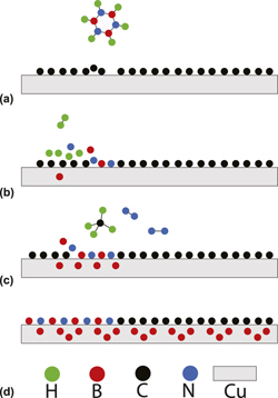
Graphene-covered copper surfaces have been exposed to borazine, (BH)3(NH)3, with the resulting surfaces characterized by low-energy electron microscopy. Although the intent of the experiment was to form hexagonal boron nitride (h-BN) on top of the graphene, such layers were not obtained. Rather, in isolated surface areas, h-BN is found to form μm-size islands that substitute for the graphene. Additionally, over nearly the entire surface, the properties of the layer that was originally graphene is observed to change in a manner that is consistent with the formation of a mixed h-BN/graphene alloy, i.e., h-BNC alloy. Furthermore, following the deposition of the borazine, a small fraction of the surface is found to consist of bare copper, indicating etching of the overlying graphene. The inability to form h-BN layers on top of graphene is discussed in terms of the catalytic behavior of the underlying copper surface and the decomposition of the borazine on top of the graphene.

Type
Invited Articles
Copyright
Copyright © Materials Research Society 2016 

Access options

Get access to the full version of this content by using one of the access options below. (Log in options will check for institutional or personal access. Content may require purchase if you do not have access.)

References

REFERENCES

Li, X., Cai, W., An, J., Kim, S., Nah, J., Yang, D., Piner, R., Velamakanni, A., Jung, I., Tutuc, E., Banerjee, S.K., Colombo, L., and Ruoff, R.S.: Large-area synthesis of high-quality and uniform graphene films on copper foils. Science 324, 1312 (2009).CrossRefGoogle ScholarPubMed
Kim, K.K., Hsu, A., Jia, X., Kim, S.M., Shi, Y., Hofmann, M., Nezich, D., Rodriguez-Nieva, J.F., Dresselhaus, M., Palacios, T., and Kong, J.: Synthesis of monolayer hexagonal boron nitride on Cu foil using chemical vapor deposition. Nano Lett. 12, 161 (2012).CrossRefGoogle ScholarPubMed
Ci, L., Song, L., Jin, C., Jariwala, D., Wu, D., Li, Y., Srivastava, A., Wang, Z.F., Storr, K., Balicas, L., Liu, F., and Ajayan, P.M.: Atomic layers of hybridized boron nitride and graphene domains. Nat. Mater. 9, 430 (2010).CrossRefGoogle ScholarPubMed
Li, X., Cai, W., Colombo, L., and Ruoff, R.S.: Evolution of graphene growth on Ni and Cu by carbon isotope labeling. Nano Lett. 9, 4268 (2009).CrossRefGoogle ScholarPubMed
Lu, G., Wu, T., Yuan, Q., Wang, H., Wang, H., Ding, F., Xie, X., and Jiang, M.: Synthesis of large single-crystal hexagonal boron nitride grains on Cu-Ni alloy. Nat. Commun. 6, 6160 (2015).CrossRefGoogle ScholarPubMed
Nagashima, A., Tejima, N., Gamou, Y., Kawai, T., and Oshima, C.: Electronic dispersion relations of monolayer hexagonal boron nitride formed on the Ni(111) surface. Phys. Rev. B: Condens. Matter Mater. Phys. 51, 4606 (1995).CrossRefGoogle ScholarPubMed
Auwärter, W., Muntwiler, M., Osterwalder, J., and Greber, T.: Defect lines and two-domain structure of hexagonal boron nitride films on Ni(111). Surf. Sci. 545, L735 (2003).CrossRefGoogle Scholar
Auwärter, W., Suter, H.U., Sachdev, H., and Greber, T.: Synthesis of one monolayer of hexagonal boron nitride on Ni(111) from B-Trichlorobrazine (ClBNH)3 . Chem. Mater. 16, 343 (2004).CrossRefGoogle Scholar
Reina, A., Jia, X., Ho, J., Nezich, D., Son, H., Bulovic, V., Dresselhaus, M.S., and Kong, J.: Large area, few-layer graphene films on arbitrary substrates by chemical vapor deposition. Nano Lett. 9, 30 (2009).CrossRefGoogle ScholarPubMed
Kang, J., Hwang, S., Kim, J.H., Kim, M.H., Ryu, J., Seo, S.J., Hong, B.H., Kim, M.K., and Choi, J.B.: Efficient transfer of large-area graphene films onto rigid substrates by hot pressing. ACS Nano 6, 5360 (2012).CrossRefGoogle ScholarPubMed
Li, X., Zhu, Y., Cai, W., Borysiak, M., Han, B., Chen, D., Piner, R.D., Colombo, L., and Ruoff, R.S.: Transfer of large-area graphene films for high-performance transparent conductive electrodes. Nano Lett. 9, 4359 (2009).CrossRefGoogle ScholarPubMed
Dan, Y., Lu, Y., Kybert, N.J., Luo, Z., and Johnson, A.T.C.: Intrinsic response of graphene vapor sensors. Nano Lett. 9, 1472 (2009).CrossRefGoogle ScholarPubMed
Roth, S., Matsui, F., Greber, T., and Osterwalder, J.: Chemical vapor deposition and characterization of aligned and incommensurate graphene/hexagonal boron nitride heterostack on Cu(111). Nano Lett. 13, 2668 (2013).CrossRefGoogle ScholarPubMed
Shi, Y., Zhou, W., Lou, A-Y., Fang, W., Lee, Y-H., Hsu, A.L., Kim, S.M., Kim, K.K., Yang, H.Y., Li, L-J., Idrobo, J-C., and Kong, J.: van der Waals epitaxy of MoS2 layers using graphene as growth templates. Nano Lett. 12, 2784 (2012).CrossRefGoogle Scholar
Yang, W., Chen, G., Shi, Z., Liu, C-C., Zhang, L., Xie, G., Cheng, M., Wang, D., Yang, R., Shi, D., Watanabe, K., Taniguchi, T., Yao, Y., Zhang, Y., and Zhang, G.: Epitaxial growth of single-domain graphene on hexagonal boron nitride. Nat. Mater. 12, 792 (2013).CrossRefGoogle ScholarPubMed
Dean, C.R., Young, A.F., Meric, I., Lee, C., Wang, L., Sorgenfrei, S., Watanabe, K., Taniguchi, T., Kim, P., Shepard, K.L., and Hone, J.: Boron nitride substrates for high-quality graphene electronics. Nat. Nanotechnol. 5, 722 (2010).CrossRefGoogle ScholarPubMed
Liu, Z., Song, L., Zhao, S., Huang, J., Ma, L., Zhang, J., Lou, J., and Ajayan, P.M.: Direct growth of graphene/hexagonal boron nitride stacked layers. Nano Lett. 11, 2032 (2011).CrossRefGoogle ScholarPubMed
Feenstra, R.M., Jena, D., and Gu, G.: Single-particle tunneling in doped graphene-insulator-graphene junctions. J. Appl. Phys. 111, 043711 (2012).CrossRefGoogle Scholar
Zhao, P., Feenstra, R.M., Gu, G., and Jena, D.: SymFET: A Proposed Symmetric Graphene Tunneling Field-Effect Transistor. IEEE Trans. Electron Devices 60, 951 (2013).CrossRefGoogle Scholar
Britnell, L., Gorbachev, R.V., Geim, A.K., Ponomarenko, L.A., Mishchenko, A., Greenaway, M.T., Fromhold, T.M., Novoselov, K.S., and Eaves, L.: Resonant tunneling and negative differential conductance in graphene transistors. Nat. Commun. 4, 1794 (2013).CrossRefGoogle ScholarPubMed
Mishchenko, A., Tu, J.S., Cao, Y., Gorbachev, R.V., Wallbank, J.R., Greenaway, M.T., Morozov, V.E., Morozov, S.V., Zhu, M.J., Wong, S.L., Withers, F., Woods, C.R., Kim, Y-J., Watanabe, K., Taniguchi, T., Vdovin, E.E., Makarovsky, O., Fromhold, T.M., Fal'ko, V.I., Geim, A.K., Eaves, L., and Novoselov, K.S.: Twist-controlled resonant tunneling in graphene/boron nitride/graphene heterostructures. Nat. Nanotechnol. 9, 808 (2014).CrossRefGoogle ScholarPubMed
Mende, P.C., Li, J., Gao, Q., Widom, M., and Feenstra, R.M.: To be published.Google Scholar
Bauer, E.: Low energy electron microscopy. Rep. Prog. Phys. 57, 895 (1994).CrossRefGoogle Scholar
Hannon, J.B. and Tromp, R.M.: Low-energy electron microscopy for nanoscale characterization. In Handbook of Instrumentation and Techniques for Semiconductor Nanostructure Characterization, Haight, R., Ross, F.M. and Hannon, J.B. eds.; World Scientific: Singapore, 2012.Google Scholar
Feenstra, R.M., Srivastava, N., Gao, Q., Widom, M., Diaconescu, B., Ohta, T., Kellogg, G.L., Robinson, J.T., and Vlassiouk, I.V.: Low-energy electron reflectivity from graphene. Phys. Rev. B: Condens. Matter Mater. Phys. 87, 041406(R) (2013).CrossRefGoogle Scholar
Srivastava, N., Gao, Q., Widom, M., Feenstra, R.M., Nie, S., McCarty, K.F., and Vlassiouk, I.V.: Low-energy electron reflectivity of graphene on copper and other substrates. Phys. Rev. B: Condens. Matter Mater. Phys. 87, 245414 (2013).CrossRefGoogle Scholar
Gao, Q., Mende, P.C., Widom, M., and Feenstra, R.M.: Inelastic effects in low-energy electron reflectivity of two-dimensional materials. J. Vac. Sci. Technol., B: Nanotechnol. Microelectron.: Mater., Process., Meas., Phenom. 33, 02B105 (2015).Google Scholar
Mende, P.C., Gao, Q., Ismach, A., Chou, H., Colombo, L., Ruoff, R.S., and Feenstra, R.M.: To be published.Google Scholar
Mende, P.C., Gao, Q., Moshin, A., Liu, L., Gu, G., and Feenstra, R.M.: To be published.Google Scholar
Hibino, H., Kageshima, H., Maeda, F., Nagase, M., Kobayashi, Y., and Yamaguchi, H.: Microscopic thickness dtermination of thin graphite films formed on SiC from quantized oscillation in reflectivity of low-energy electrons. Phys. Rev. B: Condens. Matter Mater. Phys. 77, 075413 (2008).CrossRefGoogle Scholar
Qi, Y., Rhim, S.H., Sun, G.F., Weinert, M., and Li, L.: Epitaxial graphene on SiC(0001): More than just Honeycombs. Phys. Rev. Lett. 105, 085502 (2010).CrossRefGoogle ScholarPubMed
Dhingra, S., Hsu, J-F., Vlassiouk, I., and D'Urso, B.: Chemical vapor deposition of graphene on large-domain ultra-flat copper. Carbon 69, 188 (2014).CrossRefGoogle Scholar
Vlassiouk, I., Regmi, M., Fulvio, P., Dai, S., Datskos, P., Eres, G., and Smirnov, S.: Role of hydrogen in chemical vapor deposition growth of large single-crystal graphene. ACS Nano 5, 6069 (2011).CrossRefGoogle ScholarPubMed
Święch, W., Rausenberger, B., Engel, W., Bradshaw, A.M., and Zeitler, E.: In-situ studies of heterogeneous reactions using mirror electron microscopy. Surf. Sci. 294, 297 (1993).CrossRefGoogle Scholar
Reimer, L.: Transmission Electron Microscopy, Springer Series in Optical Sciences, 4th ed., Vol. 36 (Springer, Berlin, 1997).Google Scholar
Nie, S., Wu, W., Xing, S., Yu, Q., Bao, J., Pei, S-S., and McCarty, K.F.: Growth from below: Bilayer graphene on copper by chemical vapor deposition. New J. Phys. 14, 093028 (2012).CrossRefGoogle Scholar
Koepke, J.C., Wood, J.W., Estrada, D., Ong, Z-Y., He, K.T., Pop, E., and Lyding, J.W.: Atomic-scale evidence for potential barriers and strong carrier scattering at graphene grain boundaries: A scanning tunneling microscopy study. ACS Nano 7, 75 (2013).CrossRefGoogle ScholarPubMed
Davis, L.E., MacDonald, N.C., Palmberg, P.W., Riach, G.E., and Weber, R.E.: Handbook of Auger Electron Spectroscopy, 2nd ed. (Perkin-Elmer Corporation, Eden Prairie, MN, 1978); p. 13.Google Scholar
Kidambi, P.R., Blume, R., Kling, J., Wagner, J.B., Baehtz, C., Weatherup, R.S., Schloegl, R., Bayer, B.C., and Hoffmann, S.: In-situ observations during chemical vapor deposition of hexagonal boron nitride on polycrystalline copper. Chem. Mater. 26, 6380 (2014).CrossRefGoogle ScholarPubMed
Zhang, Y., Li, Z., Kim, P., Zhang, L., and Zhou, C.: Anisotropic hydrogen etching of chemical vapor deposited graphene. ACS Nano 6, 126 (2012).CrossRefGoogle ScholarPubMed
Zhang, L., Ye, Y., Cheng, D., Pan, H., and Zhu, J.: Intercalation of Li at the graphene/Cu interface. J. Phys. Chem. 117, 9259 (2013).Google Scholar