I. INTRODUCTION
The powder-bed laser melting process is one of the most popular additive manufacturing (AM) techniques in building three-dimensional (3D) metal parts. In this process, a high-power laser beam scans on a leveled thin metal powder layer in a cold or preheated powder bed. Thermal energy provided by the laser selectively melts the metallic powder, delineating and building a 2D slice pattern based on a 3D model. A complicated 3D structure can, therefore, be fabricated via this layer-by-layer approach. The approach conserves the source materials, decreases manufacturing footprint and ancillary tooling requirements, and reduces environmental impact. Furthermore, the AM process provides agility for prototyping and design of complicated parts, reduces the cost of molds for small lot production, and has a quick turn-around time for critical in-mission repair.
In comparison to other castable aluminum (Al) alloys, silicon (Si)-modified alloys such as AlSi10Mg are an excellent choice for the AM process. The addition of Si lowers the melting point,Reference Hansen1 improves weldability and fatigue performance,Reference Brandl, Heckenberger, Holzinger and Cuchbinder2 provides excellent corrosion resistance, and ductility can be modified and improved after heat treatment. If the selected composition is close to its eutectic point, there is an 83 °C degree reduction in melting point with a narrow solidification range between liquidus and eutectic temperature for the AlSi10Mg alloy. Thus, it minimizes the required energy to melt the metal powder and permits a tighter dimensional control for building complicated shapes and overhang structures. When magnesium (Mg) is added, it can significantly enhance mechanical strengthReference Caceres, Davidson, Griffiths and Wang3 and impact performance through solution heat treatment and aging, without compromising other desirable mechanical performance aspects. These improvements are largely due to optimization of a desirable microstructure and the formation of β″ Mg2Si precipitates.Reference Jacobs4–Reference Matsuda, Naoi, Fujii, Uetani, Sato, Kamio and Ikeno6 Additional benefits such as high strength to weight ratio, sound hardness and strength, and good thermal conductivity make the Mg-modified AlSi alloys particularly attractive for automobile, aerospace, and structural applications.
When the AlSi10Mg powder is subject to a fast melting and rapid solidification in the AM process,Reference Murr7,Reference Holesinger, Carpenter, Lienert, Patterson, Papin, Swenson and Cordes8 it produces an ultrafine textured, divorced eutectic microstructure.Reference Holesinger, Carpenter, Lienert, Patterson, Papin, Swenson and Cordes8 Additionally, fast quenching rates increase the solid solubility of Si in AlReference Bose and Kumar9; therefore, it can enhance the efficacy on solution hardening and strengthening. These unique combinations imparted by the nonequilibrium process produce a superior hardness when compared to heat treated high-pressure die casting alloy parts with the same composition.Reference Mertens, Dedry, Deuter, Rigo, Lecomte-beckers and Bourell10 This work focuses on the microstructure evolution during the thermal annealing process for an AM-fabricated AlSi10Mg part. The mechanical performances such as elastic constants and microhardness associated with the thermal treatment at selected temperatures are reported. These results are associated with the microstructure evolution as the material changes from its nonequilibrium state toward its equilibrium state. Implications based on these observations are important to optimize the physical performance for solution treatable alloys used in the AM process. The impact of microstructure evolution on thermal properties of AM fabricated parts made with the AlSi10Mg alloy will be reported in a subsequent publication.Reference Yang, Deibler, Bradley, Stefan, Carroll and Jared12
II. EXPERIMENTAL PROCEDURE
A one-inch-cube part was fabricated by GPI Prototype and Manufacturing Service (Lake Bluff, IL), using AlSi10Mg powder (EOS GmbH, Krailling, Germany) and proprietary processing parameters in an EOS M280 machine. The alloyed aluminum powder consists of 9.0–11.0 wt% of Si, 0.2–0.45 wt% of Mg, <0.55 wt% of Fe, <0.45 wt% of Mn, <0.15 wt% Ti, and a trace amount of impurities including Ni, Zn, Sn, and Cu (all less than <0.1 wt%). Freshly filled and leveled powder on the XY plane (about 30 μm per layer) was selectively melted by a moving laser beam on the XY plane. Therefore, the part is built up in the +Z direction, and the in-plane and the out-of-plane refer to specimens cut from the XY and XZ planes, respectively.
Several small samples (1 × 1 × 4 mm) were sliced from the as-printed cube by a wire electrical discharge machine (EDM). Based on the differential scanning calorimetric (DSC) analysis data,Reference Yang, Deibler, Bradley, Stefan, Carroll and Jared12 a set of temperatures were selected for the annealing process. These samples were annealed in the DSC unit under flowing nitrogen to study changes in the microstructure, hardness, and elastic modulus without introducing additional oxidation. The heating and cooling rates for the annealing process were set at 20 °C per minute, and the samples were held at designated temperatures for 15 min to capture the microstructure evolution without incurring extended aging. A sample annealed at 450 °C was soaked for 30 min to ripen its microstructure for comparison purposes.
Samples for metallography were ground and polished to remove potential damage introduced by the wire EDM. An ASTM E407 #3 etchant was used to enhance the image contrast for optical and scanning electron microscopy (SEM) studies. These thermally annealed samples were immersed in the etchant for 5–10 s to preferentially remove a thin layer of aluminum and reveal the detailed microstructure of beta Si in the divorced eutectic, fusion zone (FZ), and FZ boundaries. Electron backscatter diffraction (EBSD) images were taken to study changes in grain size and morphology under different annealing conditions. The microstructural evolution of the divorced eutectic structure was studied by high-resolution SEM.
Both longitudinal and shear acoustic velocities in the X (and/or Y) and Z directions were measured at room temperature by an ultrasonic technique, using an in-house integrated system equipped with a LabView data acquisition system and an Olympus Model 5800 pulser/receiver system (Olympus NDT, Waltham, Massachusetts). Elastic constants of these specimens in different directions were calculated based on these acoustic velocities and the bulk density of the sample. Microhardness was determined via Vickers hardness measurements on polished sample surfaces, using a 0.1-kg load.
In situ X-ray analysis was performed from room temperature up to 450 °C in the XY and XZ planes to analyze the texture development, residual strain (or stress relief), and structural change. These sliced thin plates (0.5 mm in thickness) were lightly buffed with a 600 grit SiC sand paper to remove the surface layer exposed to the wire EDM. The change in lattice parameter with respect to temperature for the face centered cubic (fcc) Al was determined by standard peak fitting and lattice parameter refinement routines. The texture development induced by the AM process was measured via tilt-a-whirl methodology.Reference Rodriguez, Pearl, Van Benthem, Griego and Pillars11 The analysis for built-in residual strains for the XY and XZ planes, based on the changing in lattice spacing, was performed before and after thermal annealing. The technique used the sin2 ψ method. The Al(311) diffraction peak was monitored to determine the residual strain in the sample.
III. RESULTS AND DISCUSSION
A. Density
Using the Archimedes method, the density of the one-inch-cube of the AlSi10Mg alloy fabricated via AM is 2.671 + 0.001 g/cm3, which is slightly lower than the bulk density of the AlSi10Mg alloy (2.674 g/cm3). Data suggest that there is a small fraction of porosity in the sample, assuming oxidation of the AlSi10Mg powder is minimal during the AM process.
B. Microstructure evolution
The change of the microstructure as a function of temperature is presented in three different levels, including (i) the FZ, (ii) grain size, and (iii) the divorced eutectic cellular structure by optical microscopy, EBSD, and SEM. The specific temperatures of interest are selected by thermal analysis,Reference Yang, Deibler, Bradley, Stefan, Carroll and Jared12–Reference Fiocchi, Tuissi, Bassani and Biffi15 which are 240, 282, 307, and 450 °C. These selected temperatures correspond to the peak and the near-end temperatures from two exothermic events detected in the DSC measurement,Reference Yang, Deibler, Bradley, Stefan, Carroll and Jared12–Reference Fiocchi, Tuissi, Bassani and Biffi15 as well as the highest thermal treatment condition used in this study (i.e., 450 °C). Previous investigations of microstructural evolution have been focused on the as-fabricated AM products,Reference Holesinger, Carpenter, Lienert, Patterson, Papin, Swenson and Cordes8,Reference Prashanth, Scudino, Klauss, Surreddi, Lober, Wang, Chaubey, Kuhn and Eckert16–Reference Chou, Milligan, Paliwal and Brochu18 fast quenched samples,Reference Lavernia, Ayers and Srivastan19 and conventionally heat-treated (such as T6 treatment, >500 °C)Reference Arai, Baker, Bates, Bell, Bird, Brennan, Brooks, Brown, Caronico, Carlson, Cohen, Dahl, DeAntonio, DeArdo, Doane, Dossett, Douthett, Duhl, Ericsson, Ferguson, Filkowski, Foreman, Furchheim, Garcia, Gergely, Gilbert, Godding, Goodman, Grube, Gundlach, Hampshire, Harper, Hassell, Hensley, Hingwe, Hingwe, Howson, Jenkins, Johnson, Kirkaldy, Klaren, Knerr, Konkoly, Kovacs, Krauss, Lai, Laird, Lampman, Ludtka, Manning, McCurdy, Nelson, O'Brien, Ostrowski, Palmiere, Panzer, Pradhan, Reti, Robertson, Rohrbach, Rose, Ross, Rothman, Rowe, Ruglic, Rundman, Ryan, Sagon-King, Pierre, Sandven, Schiller, Schmidt, Shannon, Shields, Sinha, Smith, Smith, Somogyi, Stevenson, Stickels, Tenney III, Tillack, Totten, Verhoff, Walton, Webster, Wisti and Witheford20 AM parts.Reference Prashanth, Scudino, Klauss, Surreddi, Lober, Wang, Chaubey, Kuhn and Eckert16,Reference Li, Li, Liu, Zhang, Zhou, Wei, Yan and Shi21–Reference Tradowsky, White, Ward, Read, Reimers and Attallah24 The objective of these studies focused on the microstructure–mechanical property relationship before and after a conventional heat treatment. However, the microstructure evolution associated with these two exothermic reactions below 350 °C is not fully understood.Reference Yang, Deibler, Bradley, Stefan, Carroll and Jared12–Reference Fiocchi, Tuissi, Bassani and Biffi15 There are few studies devoted to the low temperature microstructure evaluation (i.e., <350 °C) for the AM produced AlSi10Mg parts. In fact, it will be shown in this study that the majority of the microstructural evolution occurs at this low temperature range.
1. Microstructure of the freezing zone
Optical images obtained at different magnifications and orientations for samples that have been thermally annealed under various temperatures are given in Fig. 1. These images are taken at 100× (scale bar = 100 µm). The microstructure delineated by the FZ boundaries on the XZ and XY surfaces exhibits a characteristic scalloped structure and a crosshatched paramecium pattern due to fast melting and rapid solidification in the direction of the laser and beam path used in the AM process. These images show that the FZ boundary, defined by the intersection of two consecutive building layers, is about 20 µm in thickness. The thickness of each FZ layer in the building direction (Z) is about 100–200 µm. These boundaries, enhanced by optical contrast due to the selective etching, exhibit coarsened Si-rich particles (or beta Si in the Al–Si binary alloy system) near each side of the boundary. This feature may be attributed to a transient, slower-growth period during the removal of latent heat from the melt poolReference Chou, Milligan, Paliwal and Brochu18 or partial remelting and coarsening of the bottom layer from the top melt pool during consecutive building processes. The majority of the pores, ranging from a few microns to tens of microns, are located near FZ boundaries and unfused regions (not shown). Although X-ray mapping by SEM shows that FZ boundaries consist of mostly Si and some Al, as well as other minor Fe impurities, other investigatorsReference Holesinger, Carpenter, Lienert, Patterson, Papin, Swenson and Cordes8 are able to detect Mg and other impurities (such as Ni, Mo, and Co) by scanning transmission electron microscopy (STEM). The shape and size of the FZ do not seem to change significantly due to annealing temperatures. However, FZ boundaries become blurred when samples are annealed above 307 °C. Images obtained after annealing at 450 °C show these FZ boundaries shrink significantly and become almost continuous thin Si lines about 1 µm in thickness. These lines eventually break into beta Si particles after further annealing.
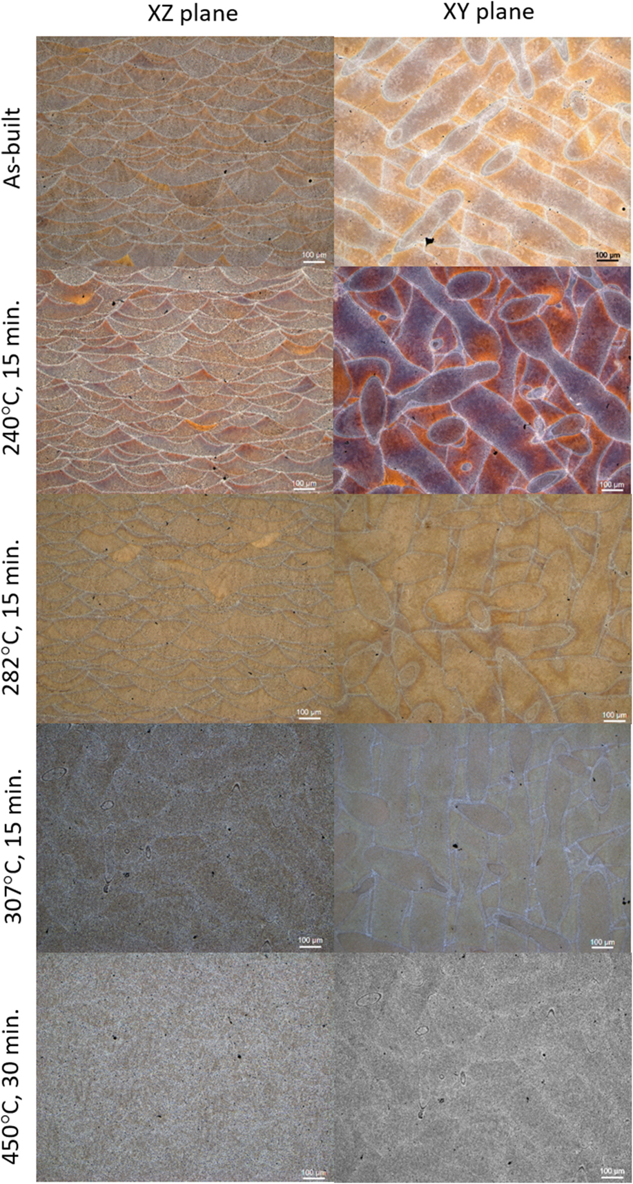
FIG. 1. Optical images of the as-built and thermally annealed AM-fabricated AlSi10Mg alloy. Images taken from the XZ plane and XY plane are given in the first and the second columns, respectively. Microphotographs for the as-built sample and thermally annealed at 240, 282, 307, and 405 °C are shown in different rows (scale bar—100 µm).
2. Grain size and morphology
Inside each FZ, there are many elongated grains more or less preferentially aligned in the build (Z) direction. These grains can be revealed by channeling contrast or EBSD technique (Fig. 2), arising from differences in crystal orientation of each grain with respect to the incident electron beam direction in the SEM. A continuous area with the same color on a color-coded EBSD image, representing a region of the same crystal orientation, defines a grain by its boundary. These elongated grains are bounded by relatively thin FZ boundaries decorated with fine black spots. These black spots are regions where the crystal orientation cannot be resolved or matched to the structure of Al. Conceivably, these FZ boundaries may consist of a high density of lattice imperfections and/or foreign materials and other phases, but the majority of these dark spots are coarsened beta Si particles as discussed in Sec. III.B.1. The elongated grains appear to nucleate from the bottom of the FZ boundary and grow preferentially in the Z direction as the solidification interface moves in an opposite direction from that of the heat transfer direction. EBSD pole figure analysis shows that the long axis of these grains within the FZ exhibits a typical (200) out-of-plane orientation for a sample sliced from XY plane (not shown), indicating that these grains are generally aligned along the 〈100〉 direction—a common easy growth direction for fcc metals.Reference Fredriksson and Akerlind26 A similar observation has been reported by many investigators.Reference Holesinger, Carpenter, Lienert, Patterson, Papin, Swenson and Cordes8,Reference Thijs, Kempen, Kruth and Van Humbeeck27 The EBSD images for the as-built sample and sample annealed at 240 °C [Figs. 2(a) and 2(b), respectively] consist of many black spots in the grains. The density of these black spots as well as the coarsened beta Si particles at the FZ boundaries progressively decreases as the temperature increases above 307 °C. These black spots found inside of Al grains at lower temperatures can be attributed to larger triple junctions of the Si cellular walls (Sec. III.B.3) or areas with a high density of dislocations and lattice imperfections induced by the rapid quenching in the AM process. A small fraction of these dark spots may also be attributed to small voids. At higher temperatures (>300 °C), these black spots are the beta Si precipitates. The length of these grains ranged from a few tens of microns to more than 200 μm. Note that the FZ boundaries also become thinner, narrower, and discontinuous at 450 °C. The average size in the length and width directions obtained from two EBSD images at each temperature are summarized in Fig. 3. Despite a large standard deviation in the image analysis, the average length and width of the grains do not seem to change significantly below 307 °C but increase moderately from 44 to 67 µm and from 14 to 16 µm at temperatures above 307 °C after the cellular wall has collapsed (Sec. III.B.3). Grain growth seems to favor the length direction perpendicular to the XY plane.
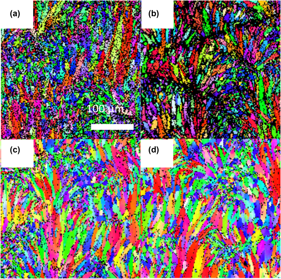
FIG. 2. Color-coded EBSD images of the as-built and thermally annealed AM-fabricated AlSi10Mg alloy. The as-built sample is shown in (a). Samples have been thermally annealed at 240, 307, and 450 °C, which are given in (b), (c), and (d) (scale bar—100 µm).

FIG. 3. Average in the length (blue) and width (red) directions of the grain structure as a function of annealing temperature determined from the EBSD images.
3. Divorced eutectic cellular structure
High-resolution SEM images in Fig. 4 show the evolution of a divorced eutectic microstructure when viewed under different thermal annealing conditions. Views are given for both XZ and XY orientations. This unique nanostructured cellular structure is produced due to rapid solidification of a hypoeutectic melt in the AM process. During this process, the oversaturated melt rejects Si and extends the solid solubility of Si into the primary Al. Consequently, it decreases the solute concentration and degree of constitutional undercooling at the solidification front, favoring the formation of a continuous, interconnected beta Si cellular wallReference Yan, Hao, Hussein, Young, Huang and Zhu17,Reference Kou25 and resulting in a divorced eutectic cellular structure.Reference Holesinger, Carpenter, Lienert, Patterson, Papin, Swenson and Cordes8,Reference Fiocchi, Tuissi, Bassani and Biffi15–Reference Tradowsky, White, Ward, Read, Reimers and Attallah24 The average cellular size in the length and width directions for the as-built sample are 1650 nm and 442 nm, respectively. The average thickness of the cellular wall is about 65 ± 21 nm. Some nanosized primary Al can be found in the thicker section of beta Si cellular walls; Mg is frequently detected by X-ray imaging in the wall areas by STEM.Reference Holesinger, Carpenter, Lienert, Patterson, Papin, Swenson and Cordes8 SEM images show that the number of nanoscale precipitates increases dramatically when the as-built sample is annealed at 240 °C for 15 min [Fig. 4(c)]. The size of most of these precipitates is 10–15 nm in diameter [Fig. 4(j)], and they are uniformly dispersed in all areas of the microstructure. The average separation between these nanoprecipitates is about 10–20 nm. The formation of these evenly distributed nanoprecipitates at low temperature is attributed to the dissolution of Si from the oversaturated primary Al cells. The excess Si in the Al lattice provides a fertile ground for nucleation and growth of precipitates.Reference Matsuda, Naoi, Fujii, Uetani, Sato, Kamio and Ikeno6,Reference Daoudi, Triki, Redjaimia and Yamina14,Reference Wahi and von Heimendahl28,Reference Wang, Esmaeili and Lloyed29 At 282 °C, the cellular walls start to collapse and break into equiaxed particles, and the density of nanosized precipitates within the Al grains decreases. Large islands at the triple wall joints break into small spherical particles, instead of growing and spheroidizing into a large particle as they normally would in an aged microstructure. The fragmentation is believed to be triggered by the formation of β′-Mg2Si,Reference Caceres, Davidson, Griffiths and Wang3,Reference Matsuda, Naoi, Fujii, Uetani, Sato, Kamio and Ikeno6,Reference Butta and Allen13,Reference Fredriksson and Akerlind26 a general strengthening agent in the AlSi10Mg alloy and will be discussed in Sec. III.D. Interestingly, these fragmented particles broken out from the cellular walls progressively align and evenly separate in lines in the solidification direction as the annealing temperature increases from 282 to 307 °C. Fiocchi et al. also observed alignment of Si particles at this temperature range and attributed this phenomenon to the disappearance of the pre-existing cellular structure.Reference Fiocchi, Tuissi, Bassani and Biffi15 Another feasible mechanism for this observation would likely be a result of a slightly better lattice matching between (200) and (220) planes of Al and Si, respectively, to minimize the local strain field between lines of particles. Further analysis at the microstructure level is needed to confirm this argument. Images captured at 307 °C also show a slight increase in size for these precipitates and particles broken from the triple junctions of cellular walls. A greater increase in precipitate size and changes in their distribution at higher temperature (>450 °C) in AM fabricated parts have also been reported.Reference Prashanth, Scudino, Klauss, Surreddi, Lober, Wang, Chaubey, Kuhn and Eckert16,Reference Li, Li, Liu, Zhang, Zhou, Wei, Yan and Shi21,Reference Aboulkhair, Maskery, Tuck, Ashcroft and Everitt23 The observed alignment disappears after the sample is annealed at 450 °C for 30 min. It is believed that the reduction of total surface energy/area becomes dominant over the lattice matching between primary Al and beta Si at the elevated temperatures. Therefore, coarsening prevails and microstructure ripens as large beta Si particles grow at the expanse of finer precipitates (i.e., Oswald ripening). The final microstructure at 450 °C resembles more or less a conventional solution treated AlSi10Mg alloy.

FIG. 4. SEM images for microstructure evolution of the divorced eutectic cellular structure for an AM-fabricated AlSi10Mg alloy. SEM images taken from the XZ plane and XY plane are given in the first and the second columns. SEM micrographs for the as-built sample [(a) and (b)] and thermally annealed at 240 °C [(c) and (d)], 282 °C [(e) and (f)], 307 °C [(g) and (h)], and 405 °C (i) are shown in different rows, including a high-resolution SEM image (j) for sample annealed at 240 °C for 15 min, showing nanosized precipitates in the cellular structure. Scale bar is given at bottom right corner.
C. Residual stress analysis
It is quite common to detect high residual stresses in large cast components with a complicated geometry,Reference Mercelis and Kruth30,Reference Vora, Mumtaz, Todd and Hopkinson31 particularly when metallic components have a high thermal expansion coefficient and a low thermal conductivity, or when parts are not adequately annealed and the casting mold and process is poorly engineered. The issue of residual stress has been an interesting subject and has been extensively studied in the AM community. Although adding Si can slightly reduce the thermal expansion coefficient and the AlSi10Mg alloy possesses a relatively high thermal conductivity in comparison to most metals, the development of an anisotropic microstructure and crystalline texture may still introduce some residual stresses in these small samples under extremely fast quenching rates.
Two samples, each cut from XY and XZ planes, were used for residual strain measurements. These strain measurements were performed before and after heating up to 450 °C for 30 min. The technique collectively measures the change in interplanar spacing (Δd/d o) of a selected diffraction peak [i.e., Al(311)] as the diffraction condition is varied from the out-of-plane condition to that of significant in-plane tilt. The results of residual strains before and after annealing at 450 °C for 30 min are given in Fig. 5. Data are reported as a function of phi (spindle axis) rotation. This means of reporting is beneficial in that it allows for the evaluation of any anisotropic variation of strain in the plane of the sample, as well as yields better assessment of the variation of strain values due to inherent error present in the sin2 ψ analysis method. The data indicate that the in-plane residual strains present in these samples are initially significant, with average values in the −0.18% range for the XY samples and −0.13 to for the XZ samples. The negative sign for strain indicates a compressive in-plane strain in the aluminum. Thermal annealing significantly decreases the strain values down to about −0.06% for both XY and XZ samples and the slight anisotropy initially observed in these samples has disappeared. The results suggest that rapid solidification in the AM process likely imparts residual stresses in the sample. These implications will be scrutinized via in situ X-ray diffraction data in Sec. III.D to shed light on the underpinning mechanism governing the observed behavior.
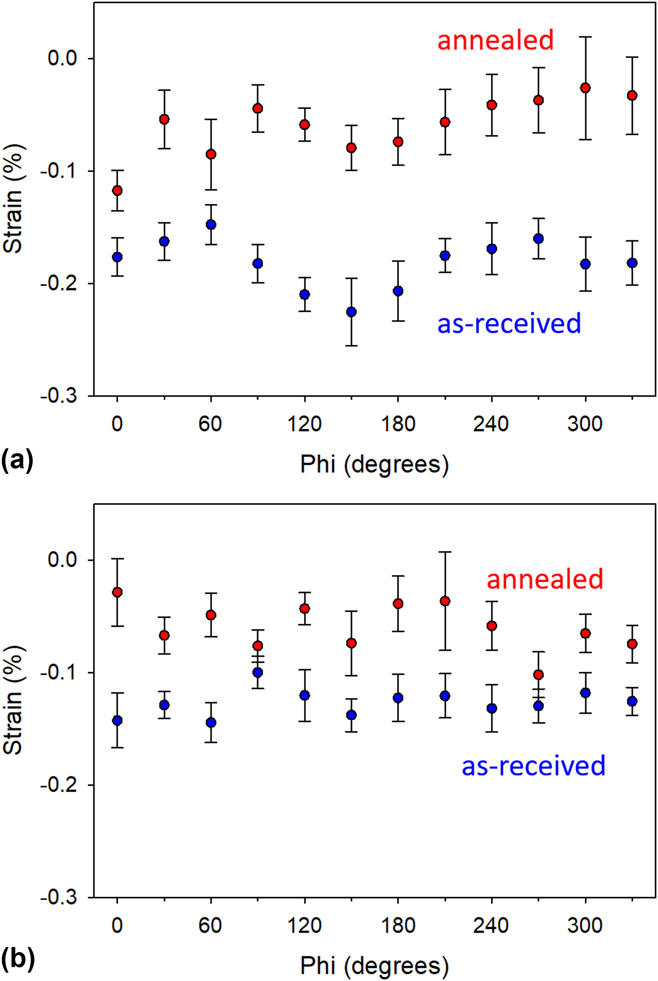
FIG. 5. Residual stain analysis based on Al(311) plane spacing measured by a tilt-a-whirl technique. (a) XY plane and (b) XZ plane.
Data collected from the tilt-a-whirl analysis can also produce pole figures to aid in the identification of texture development in the samples. Analysis results show that the XY samples have a typical (200) out-of-plane orientation, while the XZ samples have a (200) rolling texture, which might have formed via the changing of laser beam movement directions induced in the building process (not shown). There is some possible discrete nature to the fiber texture in that some of the XY pole figures for the (111) show nonuniform rings. These ring intensities appear to be more uniform in the annealed samples, suggesting that annealing at 450 °C enhances the texture development which might be attributed to the preferred anisotropic grain growth in the length (or Z) direction observed in Figs. 2(d) and 3.
D. In situ X-ray diffraction and dissolution
In situ X-ray diffraction was used to investigate changes in structure and phase evaluation from room temperature to 450 °C. Figure 6 illustrates the change of X-ray intensity of the 2θ scan as a function of temperature for the XZ specimen sliced parallel to the laser beam direction. Each temperature other than 450 °C consists of two scans, each scanning for 9 min, and at 450 °C, there are 6 scans. The heating rate was 20 °C per minute between each temperature step and the samples were heated under flowing nitrogen (150 cc/min). The peak intensity (or peak height) is represented qualitatively by the color changes on the figure where the peak intensity changes from purple (background), to blue and progressively increases all the way to the red following the visible spectrum. The figure shows that as the temperature increases, the extent of peak shift to lower 2θ angles is much greater for the Al than for Si. This simply reflects that Si has a lower coefficient of thermal expansion (2.6 × 10⁻⁶/°C) than Al (22.2 × 10⁻⁶/°C). Another interesting observation is that the relative intensity of the Al(200) peak is higher than the (111) peak, suggesting an enhanced (200) out-of-plane orientation. This is consistent with texture development in the AM fabricated part.
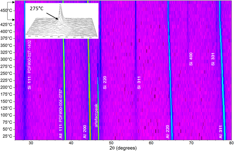
FIG. 6. In situ X-ray analysis of the XZ plane from room temperature to 450 °C for the AM-fabricated AlSi10Mg alloy. Insert figure illustrates the emerging and sharpening of the Si(111) peak.
From room temperature to 275 °C, the (111), (220), and (311) peaks for Si are rather diffuse. These Si peaks start to emerge at 150 °C, and their intensities increase rapidly above 275 °C. Above this temperature, even weaker peaks, such as (400) and (331), become noticeable. The diffuse diffraction pattern observed at low temperatures is indicative of the presence of an ultrafine crystallite size (less than 100 nm) for Si, which is consistent with the nanosized cellular structure and the ultrafine Si precipitates reported in Sec. III.C [Figs. 4(a) and 4(c)]. At higher temperatures (>275 °C), the diffraction peaks sharpen, indicating the coarsening of Si precipitates in the AlSi10Mg alloy. The in situ X-ray diffraction measurement, thus, illustrates the dissolution and coarsening of Si from the oversaturated Al lattice imparted by rapid quenching in the heating process and is supported by the microstructure evolution presented in Sec. III.B.3.
Note that the 2θ angles between the (200) and (220) of Al and Si planes are closer than any other planes. This can provide a closer lattice matching and less lattice strain at local scale between the fine Si precipitates and primary Al matrix and has been reported to develop a coherent yet strained interface in the AlSi10Mg alloy by several high-resolution transmission electron microscopy studies.Reference Matsuda, Naoi, Fujii, Uetani, Sato, Kamio and Ikeno6,Reference Holesinger, Carpenter, Lienert, Patterson, Papin, Swenson and Cordes8,Reference Butta and Allen13 Therefore, near 300 °C [Figs. 4(e) and 4(g)], when cellular walls, preferentially aligned in the solidification direction, become thermally unstable, the Al(200) planes could provide a better lattice match with Si(220) planes at local scale. As the temperature increases, the 2θ angles between Al(200) and Si(220) increase (Fig. 6), resulting in a higher lattice strain between primary Al and Si cellular walls. By breaking these walls into smaller particles, the local strain due to lattice mismatch can be reduced. After these walls break up, Si atoms may once again migrate and form beta Si particles aligning perpendicular to the Al(200) planes and evenly spread in the microstructure to minimize the lattice strain energy. Further study will be helpful to evaluate the proposed hypothesis.
The lattice parameter refinement of data collected in Fig. 6 shows a change in the Al lattice parameter as a function of temperature for the as-built specimen (see Fig. 7). This figure shows two linear regions, i.e., between room temperature and 125 °C, and from 275 to 450 °C. Error bars in Fig. 7 are plotted using 3 standard deviations of the reported a-axis parameter error; therefore, the deviations observed from measurements appear significant. The linear response observed in the low temperature section reflects the thermal expansion coefficient of the as-built part (i.e., 2.57 × 10⁻⁵/°C) where thermally induced diffusion is limited. The slight deviation from linearity between 125 and 275 °C can be further divided into two sections. In the first section between 125 and 200 °C, the unit cell expands at a faster rate than a typical linear thermal expansion would dictate. From 200 to 275 °C, the expansion undergoes another slope change where the Al lattice expands at a slower rate compared to the expected thermal expansion rate until 275 °C where the thermal expansion becomes linear again. This observation is in good agreement with the thermomechanical response measured via dilatometry.Reference Yang, Deibler, Bradley, Stefan, Carroll and Jared12 The expansion of the unit cell is consistent with the dissolution of smaller Si atoms from an oversaturated Al lattice as observed in the SEM (Fig. 4) and in situ X-ray study (Fig. 6) and is supported by the aforementioned extended Si solubility in primary Al phase during the eutectic cellular structure formation in the as-built part. The reduced thermal expansion region between 200 and 275 °C is most likely due to the dissolution of slightly larger Mg atoms from the primary Al lattice. Although there is no direct evidence in this study, we foresee that the dissolution of Mg aids the formation of β′-Mg2Si—a key strengthening agent for the improvement of mechanical strength of AlSi10Mg alloys. DSCReference Matsuda, Naoi, Fujii, Uetani, Sato, Kamio and Ikeno6,Reference Yang, Deibler, Bradley, Stefan, Carroll and Jared12–Reference Fiocchi, Tuissi, Bassani and Biffi15 and TEM studiesReference Matsuda, Naoi, Fujii, Uetani, Sato, Kamio and Ikeno6,Reference Butta and Allen13,Reference Daoudi, Triki, Redjaimia and Yamina14 confirm that this temperature range is consistent with β′-Mg2Si formation. Additionally, it is quite plausible in this temperature range that the slightly higher Mg concentration in the cellular wallReference Holesinger, Carpenter, Lienert, Patterson, Papin, Swenson and Cordes8 will be ready to react with Si and form β′-Mg2Si, thereby, triggering the cellular wall collapse and preventing the formation of large spherical particles at the triple wall junctions as illustrated in Figs. 4(e)–4(h). Once these excess foreign atoms diffuse out from the primary Al lattice, a linear thermal expansion is restored (3.49 × 10⁻⁵/°C between 300 and 450 °C).
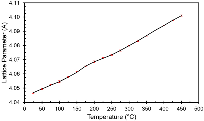
FIG. 7. X-ray structural refinement for the lattice parameter of Al in the as-built part as a function of temperature.
The refined lattice parameters obtained for the XY and XZ samples in the as-built state were 4.0444(2) Å and 4.0475(7) Å, respectively. After cooling down from the in situ measurement, the lattice parameter increased to 4.0506(1) for both the XY and XZ parts. This is still slightly smaller than the pure Al, indicating that there is a limited solubility of Si in the primary alpha Al phase in the AlSi10Mg alloy and gives further support to the Si dissolution argument. The observed difference in lattice spacing from different directions immediately suggests that the in-plane direction might have a higher residual compressive stress since the lattice parameter for pure aluminum is 4.0509(5) Å (PDF entry 00-004-0787). This is consistent with the residual strain analysis based on the (311) plane in Sec. III.C. However, the lattice spacing can also vary with solute concentration in a solid solutionReference Bose and Kumar9,Reference Li, Li, Liu, Zhang, Zhou, Wei, Yan and Shi21 ; if this argument is indeed true for this study case, the anisotropy found in lattice spacing suggests that Si will be more likely to substitute in the Al lattice perpendicular to the solidification direction in the AM process. This argument is self-consistent with the observation of Si dissolution and thermal expansion behavior as determined by the lattice parameter refinement of the Al phase from the in situ X-ray diffraction data. Therefore, the “apparent” residual stresses observed by the change of lattice spacing could be misleading for small samples investigated in this study. However, parts built with complex geometries, size, those anchored on rigid substrates, or processed with different parameters can still develop residual stresses due to thermomechanical stresses.
E. Elastic moduli and microhardness
The change of elastic moduli as a function of temperature was determined by acoustic velocity measurements for the samples that had been annealed at different temperatures. Both longitudinal and transverse shear velocities are measured in the directions parallel and perpendicular to the build direction. Surprisingly, it is found that the differences in acoustic velocity and elastic stiffness of these directions are less than 1.8%, particularly considering the difference in texture and microstructure in these samples. Moreover, the fact that the difference in shear velocities measured parallel (Z) and perpendicular (X or Y) to build direction are less than 1% suggests that these samples are almost elastically isotropic in mechanical response. Therefore, calculated elastic constants such as Young’s modulus, shear modulus, and Poisson’s ratio based on acoustic velocity measurements should be close to the elastic properties of the AM parts. The results of the elastic properties for these samples annealed at different temperatures are given in Fig. 8(a). To reflect the fact that there is still a slight difference in acoustic velocity observed in different directions, quotation marks are added to these elastic constants. Data indicate that both “Young’s modulus” and “shear modulus” do not change significantly for the samples that have been annealed above 240 °C for more than 15 min. The “Young’s modulus” and “shear modulus” of these samples are 78.4 GPa and 29.2 GPa, respectively. Note that elastic constants of the as-built sample are lower. The “Young’s modulus” for the as-built samples is around 74 GPa, which is consistent with acoustic measurement data reported by other investigators.Reference Thijs, Kempen, Kruth and Van Humbeeck27 The fundamental reason for this unusual observation is not clear. However, it must correlate with the oversaturated Si atoms in the Al lattice due to rapid quenching of the AlSi10Mg alloy. When nanosized Si precipitates form above 240 °C, these elastic constants (or bonding strength) restore and hold almost constant regardless of the sample’s thermal history. Further investigation and computational modeling are needed to understand the observed behavior.
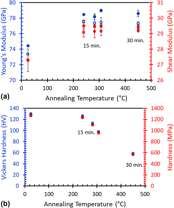
FIG. 8. Summary of elastic property measurements. (a) Elastic “moduli” measurement determined by acoustic measurement for the samples annealed at different temperatures and times. Blue legend and red legend are “Young’s” modulus and “shear” modulus, respectively. The solid and open circles are the data collected in the Z and X directions. (b) Vickers hardness of the AM-fabricated AlSi10Mg samples annealed at different temperatures and times.
The change of microhardness for the samples that have been annealed at different temperatures is measured by Vickers indentation and the results are given in Fig. 8(b). The as-built part possesses a superior hardness which agrees with published data. The Vickers hardness measured for the as-built sample is twice that of the sample annealed at 450 °C for 30 min and is also greater than wrought and cast aluminum alloys commonly utilized in traditional manufacturing.Reference Mertens, Dedry, Deuter, Rigo, Lecomte-beckers and Bourell10 The progressive decrease in microhardness with respect to increased annealing temperature is correlated with the microstructure evolution and mechanisms hindering the dislocation motion in the material. Common known mechanisms that can effectively hinder the dislocation motion in a plastic deformation include solution hardening, precipitation hardening, and grain boundaries, as well as entangled high-density dislocations due to plastic deformation. Depending on their size, length scale in separation, and distribution, some mechanisms may not be effective in hindering dislocation motion in a localized plastic deformation induced by a microindenter. For example, the distance between FZ boundaries and grain boundaries will not play an important role due to their relative length scale (greater than a few tens of microns) in comparison with the travel distance of dislocations. The argument is further supported by the microhardness measurement in the XY and XZ planes, where the difference and the standard deviation between the measured values from these two planes are small and almost indistinguishable, despite the large difference in their microstructure. Previous workReference Aboulkhair, Tuck, Ashcroft, Maskery and Everit22 has attributed the observed superior hardness to the increased volume of grain boundaries due to rapid quenching, but our study has shown that the grain size does not change significantly below 307 °C and only increases moderately after being annealed at 450 °C for 30 min. On the other hand, solution hardening, uniformly dispersed precipitates, and cellular walls in a divorced eutectic microstructure, all in the nanoscale region, can act as effective obstacles for dislocation motion. In comparison to the microstructure of the as-built sample and the sample annealed at 240 °C, solution hardening due to oversaturated Al lattice appears to be the major contributor to its superior hardness found in the as-built sample, as cellular walls still remain intact for both conditions. Dislocation motion will be constantly counteracting with high-density lattice imperfections, such as solute atoms, lattice strains due to lattice mismatching, and entangled dislocations induced by rapid quenching, just to name a few, in the as-built part. At 240 °C, Si aggregates and forms precipitates and the density of these obstacles decreases; therefore, its hardness decreases slightly. From 240 to 282 °C, in accordance with the expectation, these nanosize precipitates grow and their density decreases, and eventually the cellular wall fragments into fine particles as the microhardness continues declining up to 307 °C. When these interconnected cellular walls collapse after the sample has been annealed and slightly overaged at 450 °C for 30 min, the length scale and probability of encountering large beta Si particles by dislocation motion is significantly decreased, therefore, depressing the effect of precipitate hardening. In comparison to the sample that is annealed at 240 °C, the microhardness reduces to almost half of its original value. This dramatic change highlights the important contribution of a continuous nanoscale cellular structure to the microhardness as it has also been recognized by other studies.Reference Yan, Hao, Hussein, Young, Huang and Zhu17,Reference Brito, Reinhart, Nguyen-Thi, Mangelinck-Noel, Cheung, Spinelli and Garcia32
Several interesting scientific phenomena have been observed, including the self-alignment of beta silicon particles broken from the collapsing of the cellular structure near 300 °C and the decreasing of elastic modulus in the oversaturated, nonequilibrium AlSi10Mg alloy. These observations will be further studied by computational modeling and simulation to shed light on the unpinning mechanism of these behaviors. Additionally, the evaluation of few mechanical properties directly relevant to practical engineering applications, such as yield strength, elongation, and ultimate strength as a function of heat treatment will be an interesting subject for future studies. The implication of microstructure evolution on thermal properties due to the change in length scale for electron and photon scattering will be reported in a companioned publication.Reference Yang, Deibler, Bradley, Stefan, Carroll and Jared12
IV. SUMMARY
This publication summarizes the microstructure evolution during thermal annealing of an AM-fabricated AlSi10Mg part. Because of the rapid solidification involved in the AM process, the sample locks in a nonequilibrium state and exhibits unique textured, elongated grains with an ultrafine divorced cellular structure. As the temperature increases and the material progressively approaches its equilibrium, a sequential change develops, including Si dissolution, precipitation, collapsing of the cellular structure, and microstructure ripening. The dissolution and microstructural evolution effectively change the size, morphology, length scale, and distribution of nanosized precipitates and cellular structure and have a profound effect on mechanical properties as demonstrated by the change in microhardness. For a relatively small sample used in this study, the change in lattice spacing in the as-built sample, determined by lattice parameter refinement and residual stress analysis, can be attributed to the oversaturated Si in the primary Al lattice due to rapid quenching in the AM process; not due to residual stresses commonly reported in the literature. This is supported and demonstrated by the dissolution of Si by the microstructural evolution and in situ X-ray diffraction studies. Before microstructural ripening occurs, the fragmented beta Si from the divorced cellular wall tends to align with the solidification direction to minimize the overall lattice strain energy in the sample. Issues related to the nonequilibrium states imparted by the AM process should not be unique to the AlSi10Mg alloy. Observations reported in this study could have important implications to other popular, solution treatable alloys such as Inconel 718 and Ti6Al4V fabricated by the AM process.
ACKNOWLEDGMENTS
The authors would like to thank Michael Saavedra for sample preparation and Deidre Hirschfeld for programmatic support. Sandia National Laboratories is a multimission laboratory managed and operated by National Technology and Engineering Solutions of Sandia, LLC, a wholly owned subsidiary of Honeywell International, Inc., for the U.S. Department of Energy’s National Nuclear Security Administration under contract DE-NA0003525.


