Hostname: page-component-745bb68f8f-hvd4g Total loading time: 0 Render date: 2025-01-26T01:40:29.684Z Has data issue: false hasContentIssue false

The effect of substrate pore size on the network interconnectivity and electrical properties of dropcasted multiwalled carbon nanotube thin films

Published online by Cambridge University Press:  07 June 2013

Rachel L. Muhlbauer
Affiliation:
School of Materials Science and Engineering, Georgia Institute of Technology, Atlanta, Georgia 30332-0245
Salil M. Joshi
Affiliation:
School of Materials Science and Engineering, Georgia Institute of Technology, Atlanta, Georgia 30332-0245
Rosario A. Gerhardt*
Affiliation:
School of Materials Science and Engineering, Georgia Institute of Technology, Atlanta, Georgia 30332-0245
*
a)Address all correspondence to this author. e-mail: [email protected]
Get access

Abstract

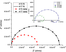
Four-layer multiwalled carbon nanotube (MWNT) thin films were deposited via dropcasting (1 mg/mL MWNTs and 10 mg/mL SDBS) onto filter papers that vary in pore size (1, 5, 25, and 40 µm) to determine the effect of the underlying substrate structure on the in-plane properties of the films. The films (<100 nm thick) were dried using vacuum filtration, and drying in a 65 °C heater with and without a ceramic heating board. DC resistance of the films ranged from 6 × 10³ to 9.3 × 10⁹ Ω. Impedance spectroscopy analysis revealed a low and a high frequency inductive response and two parallel R–C circuits for the more conducting thin films. High resistance films were fit by a single RC circuit with a constant-phase element. The differences in the in-plane electrical responses of the different MWNT films can be explained by the degree of carbon nanotube surface coverage, obtained as a result of using different pore size filter papers. The drying method utilized also affected the CNT network formation and its resultant electrical properties.

Type
Articles
Copyright
Copyright © Materials Research Society 2013 

Access options

Get access to the full version of this content by using one of the access options below. (Log in options will check for institutional or personal access. Content may require purchase if you do not have access.)

References

REFERENCES

Iijima, S.: Helical microtubules of graphitic carbon. Nature 354, 56 (1991).CrossRefGoogle Scholar
Iijima, S. and Ichihashi, T.: Single-shell carbon nanotubes of 1-nm diameter. Nature 363, 603 (1993).CrossRefGoogle Scholar
Zhang, W., Zhu, Z., Wang, F., Wang, T., Sun, L., and Wang, Z.: Chirality dependence of the thermal conductivity of carbon nanotubes. Nanotechnology 15, 936 (2004).CrossRefGoogle Scholar
Wei, B.Q., Vajtai, R., and Ajayan, P.M.: Reliability and current carrying capacity of carbon nanotubes. Appl. Phys. Lett. 79, 1172 (2001).CrossRefGoogle Scholar
Hu, L., Hecht, D.S., and Gruner, G.: Carbon nanotube thin films: Fabrication, properties, and applications. Chem. Rev. 110, 5790 (2010).CrossRefGoogle ScholarPubMed
Gruner, G.: Carbon nanotube films for transparent and plastic electronics. J. Mater. Chem. 16, 3533 (2006).CrossRefGoogle Scholar
Zhu, H., Wei, J., Wang, K., and Wu, D.: Applications of carbon materials in photovoltaic solar cells. Sol. Energy Mater. Sol. Cells 93, 1461 (2009).CrossRefGoogle Scholar
Muhlbauer, R.L. and Gerhardt, R.A.: A review on the synthesis of carbon nanotube thin films, in Carbon Nanotubes: Synthesis and Properties, edited by A.K. Mishra (Nova Science Publishers, Happauge, NY, 2012), pp. 107156.Google Scholar
Yang, K., He, J., Puneet, P., Su, Z., Skove, M.J., Gaillard, J., Tritt, T.M., and Rao, A.M.: Tuning electrical and thermal connectivity in multiwalled carbon nanotube buckypaper. J. Phys. Condens. Matter. 22, 334215 (2010).CrossRefGoogle ScholarPubMed
Huang, L., Chen, K., Peng, C., and Gerhardt, R.A.: Highly conductive paper fabricated with multiwalled carbon nanotubes and poly(3,4-ethylenedioxythiophene)-poly(styrenesulfonate) by unidirectional drying. J. Mater. Sci. 46, 6648 (2011).CrossRefGoogle Scholar
Hu, L., Choi, J.W., Yang, Y., Jeong, S., La Mantia, F., Cui, L-F., and Cui, Y.: Highly conductive paper for energy-storage devices. PNAS 106, 21490 (2009).CrossRefGoogle ScholarPubMed
Tobjork, D. and Osterbacka, R.: Paper electronics. Adv. Mater. 23, 1935 (2011).CrossRefGoogle ScholarPubMed
Barr, M.C., Rowehl, J.A., Lunt, R.R., Xu, J., Wang, A., Boyce, C.M., Im, S.G., Bulovic, V., and Gleason, K.K.: Direct monolithic integration of organic photovoltaic circuits on unmodified paper. Adv. Mater. 23, 3500 (2011).CrossRefGoogle ScholarPubMed
Lyth, S.M. and Silva, S.R.P.: Field emission from multiwall carbon nanotubes on paper substrates. Appl. Phys. Lett. 90, 173124 (2007).CrossRefGoogle Scholar
Kordas, K., Mustonen, T., Toth, G., Jantunen, H., Lajunen, M., Soldano, C., Talapatra, S., Kar, S., Vajtai, R., and Ajayan, P.M.: Inkjet printing of electrically conductive patterns of carbon nanotubes. Small 2, 1021 (2006).CrossRefGoogle ScholarPubMed
Muhlbauer, R.L and Gerhardt, R.A.: Impedance spectroscopy of short multiwalled carbon nanotube networks deposited on a paper substrate: The evolution of in-plane and thru-plane properties. App. Phys. Lett. Submitted.Google Scholar
de Heer, W.A., Bacsa, W.S., Chatelain, A., Gerfin, T., Humphrey-Baker, R., Forro, L., and Ugarte, D.: Aligned carbon nanotube films: Production and optical and electronic properties. Science 268, 845 (1995).CrossRefGoogle Scholar
Macdonald, J.R.: Impedance spectroscopy. Ann. Biomed. Eng. 20, 289 (1992).CrossRefGoogle ScholarPubMed
Gerhardt, R.A: Impedance and mobility spectra, in Encyclopedia of Condensed Matter Physics, edited by F. Bassani, G.L. Liedl and P. Wyder (Elsevier, New York, 2005), p. 350.CrossRefGoogle Scholar
Joshi, S.M. and Gerhardt, R.A.: Effect of annealing atmosphere (air vs. argon) and temperature on the electrical properties of spin coated colloidal indium tin oxide films. J. Mater. Sci. 48(3), 1465 (2013).CrossRefGoogle Scholar
Kumar, V.S., Kelekanjeri, G., and Gerhardt, R.A.: Characterization of microstructure fluctuations in Waspaloy exposed to 760 °C for times up to 2500 h. Electrochim. Acta 51, 1873 (2006).Google Scholar
Garrett, M.P., Ivanov, I.N., Gerhardt, R.A., Puretsky, A.A., and Geohegan, D.B.: Separation of junction and bundle resistance in single wall carbon nanotube percolation networks by impedance spectroscopy. Appl. Phys. Lett. 97, 163105 (2010).CrossRefGoogle Scholar
Louie, S.G.: Electronic properties, junctions, and defects of carbon nanotubes, in Carbon Nanotubes: Synthesis, Structure, Properties, and Applications, Vol. 80, edited by M.S. Dresselhaus, G. Dresselhaus and P. Avouris (Springer, Berlin, 2001), p. 113.CrossRefGoogle Scholar
Hecht, D., Hu, L., and Gruner, G.: Conductivity scaling with bundle length and diameter in single walled carbon nanotube networks. Appl. Phys. Lett. 89, 133112 (2006).CrossRefGoogle Scholar
Nirmalraj, P.N., Lyons, P.E., De, S., Coleman, J.N., and Boland, J.J.: Electrical conductivity in single-walled carbon nanotube networks. Nano Lett. 9, 3890 (2009).CrossRefGoogle Scholar
Capozzi, C.J. and Gerhardt, R.A.: Correlation of the ac electrical conductivity and the microstructure of PMMA/ITO nanocomposites that possess phase-segregated microstructures. J. Phys. Chem. C 112, 19372 (2008).CrossRefGoogle Scholar
Bertram, B.D., Gerhardt, R.A., and Schultz, J.W.: Impedance response and modeling of composites containing aligned semiconductor whiskers: Effects of dc-bias partitioning and percolated-cluster length, topology, and filler interfaces. J. Appl. Phys. 111, 124913 (2012).CrossRefGoogle Scholar
Brug, G.J., van den Eeden, A.L.G., Sluyters-Rehbach, M., and Sluyters, J.H.: The analysis of electrode impedances complicated by the presence of a constant phase element. J. Electroanal. Chem. Interfacial Electrochem. 176, 275 (1984).CrossRefGoogle Scholar