Hostname: page-component-cd9895bd7-fscjk Total loading time: 0 Render date: 2025-01-04T06:08:31.865Z Has data issue: false hasContentIssue false

Effect of annealing temperature on the electrical characteristics of Ti–Zn–Sn–O thin-film transistors fabricated via a solution process

Published online by Cambridge University Press:  18 May 2012

Jong Chil Do
Affiliation:
School of Materials Science and Engineering, Kyungpook National University, Daegu 702-701, Korea
Ho Beom Kim
Affiliation:
School of Materials Science and Engineering, Kyungpook National University, Daegu 702-701, Korea
Cheol Hyoun Ahn
Affiliation:
School of Advanced Materials Science and Engineering, Sungkyunkwan University, Suwon 440-746, Korea
Hyung Koun Cho
Affiliation:
School of Advanced Materials Science and Engineering, Sungkyunkwan University, Suwon 440-746, Korea
Ho Seong Lee*
Affiliation:
School of Materials Science and Engineering, Kyungpook National University, Daegu 702-701, Korea
*
a)Address all correspondence to this author. e-mail: [email protected]
Get access

Abstract

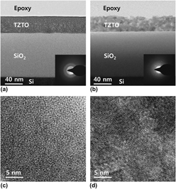
Thin-film transistors (TFTs) utilizing a TiZnSnO (TZTO) channel layer were fabricated by using a solution process. The effect of annealing temperature on the device performance of the TZTO TFTs was investigated. TFTs with nanocrystalline TZTO films exhibited a better device performance than those with amorphous TZTO films. The on/off current ratio of the TZTO TFTs annealed at 600 °C was as large as 4.2 × 10⁶. The field-effect mobility (μFE) of 4.1 cm2/Vs and subthreshold swing of 1.2 V/decade were achieved.

Type
Articles
Copyright
Copyright © Materials Research Society 2012

Access options

Get access to the full version of this content by using one of the access options below. (Log in options will check for institutional or personal access. Content may require purchase if you do not have access.)

References

REFERENCES

1.Frenzel, H., Lajn, A., von Wenckstern, H., Lorenz, M., Schein, F., Zhang, Z., and Grundmann, M.: Recent progress on ZnO-based metal-semiconductor field-effect transistors and their application in transparent integrated circuits. Adv. Mater. 22, 5332 (2010).CrossRefGoogle ScholarPubMed
2.Ozgur, U., Alivov, Ya.I., Liu, C., Teke, A., Reshchikov, M.A., Dogan, S., Avrutin, V., Cho, S.J., and Morkoc, H.: A comprehensive review of ZnO materials and devices. J. Appl. Phys. 98, 041301 (2005).CrossRefGoogle Scholar
3.Lee, S. and Paine, D.C.: On the effect of Ti on the stability of amorphous indium zinc oxide used in thin film transistor applications. Appl. Phys. Lett. 98, 262108 (2011).CrossRefGoogle Scholar
4.Chiang, H.Q., Wager, J.F., Hoffman, R.L., Jeong, J., and Keszler, D.A.: High mobility transparent thin-film transistors with amorphous zinc tin oxide channel layer. Appl. Phys. Lett. 86, 013503 (2005).CrossRefGoogle Scholar
5.Seo, S.J., Choi, C.G., Hwang, Y.H., and Bae, B.S.: High performance solution-processed amorphous zinc tin oxide thin film transistor. J. Phys. D: Appl. Phys. 42, 035106 (2009).CrossRefGoogle Scholar
6.Nomura, K., Ohta, H., Takagi, A., Kamiya, T., Hirano, M., and Hosono, H.: Room-temperature fabrication of transparent flexible thin-film transistors using amorphous oxide semiconductors. Nature 432, 488 (2004).CrossRefGoogle ScholarPubMed
7.Sung, S.Y., Choi, J.H., Han, U.B., Lee, K.C., Lee, J.H., Kim, J.J., Lim, W., Pearton, S.J., Norton, D.P., and Heo, Y.W.: Effects of ambient atmosphere on the transfer characteristics and gate-bias stress stability of amorphous indium-gallium-zinc oxide thin-film transistors. Appl. Phys. Lett. 96, 102107 (2010).CrossRefGoogle Scholar
8.Jeong, J.K., Jeong, J.H., Yang, H.W., Park, J.S., Mo, Y.G., and Kim, H.D.: High performance thin film transistors with cosputtered amorphous indium gallium zinc oxide channel. Appl. Phys. Lett. 91, 113505 (2007).CrossRefGoogle Scholar
9.Jeong, Y., Song, K., Kim, D., Koo, C.Y., and Moon, J.: Bias stress stability of solution-processed zinc tin oxide thin-film transistors. J. Electrochem. Soc. 156, H808 (2009).CrossRefGoogle Scholar
10.Jeong, Y., Bae, C., Kim, D., Song, K., Woo, K., Shin, H., Cao, G., and Moon, J.: Bias-stress-stable solution-processed oxide thin film transistors. ACS Appl. Mater. Interfaces 2, 611 (2010).CrossRefGoogle ScholarPubMed
11.Maeng, W.J., Park, J.S., Kim, H.S., Lee, K.H., Park, K.B., Son, K.S., Kim, T.S., Kim, E.S., Ham, Y.N., Ryu, M., and Lee, S.Y.: Photo and thermal stability enhancement of amorphous Hf-In-Zn-O thin-film transistors by the modulation of back channel composition. Appl. Phys. Lett. 98, 073503 (2011).CrossRefGoogle Scholar
12.Yang, B.S., Huh, M.S., Oh, S., Lee, U.S., Kim, Y.J., Oh, M.S., Jeong, J.K., Hwang, C.S., and Kim, H.J.: Role of ZrO2 incorporation in the suppression of negative bias illumination-induced instability in Zn-Sn-O thin film transistors. Appl. Phys. Lett. 98, 122110 (2011).CrossRefGoogle Scholar
13.Seo, S.J., Jeon, J.H., Hwang, Y.H., and Bae, B.S.: Improved negative bias illumination instability of sol-gel gallium zinc tin oxide thin film transistors. Appl. Phys. Lett. 99, 152102 (2011).CrossRefGoogle Scholar
14.Kwon, D.W., Kim, J.H., Chang, J.S., Kim, S.W., Kim, W., Park, J.C., Song, I., Kim, C.J., Jung, U.I., and Park, B.G.: Temperature effect on negative bias-induced instability of HfInZnO amorphous oxide thin film transistor. Appl. Phys. Lett. 98, 063502 (2011).CrossRefGoogle Scholar
15.Rim, Y.S., Kim, D.L., Jeong, W.H., and Kim, H.J.: Effect of Zr addition on ZnSnO thin-film transistors using a solution process. Appl. Phys. Lett. 97, 233502 (2010).CrossRefGoogle Scholar
16.Ahn, C.H., Kim, Y.Y., Kang, S.W., Kong, B.H., Mohante, S.K., Cho, H.K., Kim, J.H., and Lee, H.S.: Dependence of oxygen partial pressure on the characteristics of ZnO films grown by radio frequency magnetron sputtering. J. Mater. Sci. - Mater. Electron. 19, 744 (2008).CrossRefGoogle Scholar
17.Ryu, M.K., Yang, S., Park, S.H.K., Hwang, C.S., and Jeong, J.K.: High performance thin film transistor with cosputtered amorphous Zn-In-Sn-O channel: Combinatorial approach. Appl. Phys. Lett. 95, 072104 (2009).CrossRefGoogle Scholar
18.Song, K., Noh, J., Jun, T., Jung, Y., Kang, H.Y., and Moon, J.: Fully flexible solution-deposited ZnO thin-film transistors. Adv. Mater. 22, 4308 (2010).CrossRefGoogle ScholarPubMed
19.Kim, G.H., Jeong, W.H., Ahn, B.D., Shin, H.S., Kim, H.J., Kim, H.J., Ryu, M.K., Park, K.B., Seon, J.B., and Lee, S.Y.: Investigation of the effects of Mg incorporation into InZnO for high-performance and high-stability solution-processed thin film transistors. Appl. Phys. Lett. 96, 163506 (2010).CrossRefGoogle Scholar
20.Chong, H.Y., Han, K.W., No, Y.S., and Kim, T.W.: Effect of the Ti molar ratio on the electrical characteristics of titanium-indium-zinc-oxide thin-film transistors fabricated by using a solution process. Appl. Phys. Lett. 99, 161908 (2011).CrossRefGoogle Scholar
21.Cho, D.H., Yang, S., Byun, C., Shin, J., Ryu, M.K., Park, S.H.K., Hwang, C.S., Chung, S.M., Cheong, W.S., Yoon, S.M., and Chu, H.Y.: Transparent Al-Zn-Sn-O thin film transistors prepared at low temperature. Appl. Phys. Lett. 93, 142111 (2008).CrossRefGoogle Scholar
22.Kim, G.H., Shin, H.S., Ahn, B.D., Kim, K.H., Park, W.J., and Kim, H.J.: Formation mechanism of solution-processed nanocrystalline InGaZnO thin film as active channel layer in thin-film transistor. J. Electrochem. Soc. 156, H7 (2009).CrossRefGoogle Scholar
23.Seo, S.J., Hwang, Y.H., and Bae, B.S.: Postannealing process for low temperature processed sol-gel zinc tin oxide thin film transistors. Electrochem. Solid-State Lett. 13, H357 (2010).CrossRefGoogle Scholar
24.Kwon, D.W., Kim, J.H., Chang, J.S., Kim, S.W., Sun, M.C., Kim, G., Kim, H.W., Park, J.C., Song, I., Kim, C.J., Jung, U.I., and Park, B.G.: Charge injection from gate electrode by simultaneous stress of optical and electrical biases in HfInZnO amorphous oxide thin film transistor. Appl. Phys. Lett. 97, 193504 (2010).CrossRefGoogle Scholar
25.Kwon, J.Y., Jung, J.S., Son, K.S., Lee, K.H., Park, J.S., Kim, T.S., Park, J.S., Choi, R., Jeong, J.K., Koo, B., and Lee, S.: Investigation of light-induced bias instability in Hf-In-Zn-O thin film transistors: A cation combinatorial approach. J. Electrochem. Soc. 158, H433 (2011).CrossRefGoogle Scholar
26.Kim, G.H., Ahn, B.D., Shin, H.S., Jeong, W.H., Kim, H.J., and Kim, H.J.: Effect of indium composition ratio on solution-processed nanocrystalline InGaZnO thin film transistors. Appl. Phys. Lett. 94, 233501 (2009).CrossRefGoogle Scholar
27.Ong, B.S., Li, C., Li, Y., Wu, Y., and Loutfy, R.: Stable, solution-processed, high-mobility ZnO thin-film transistors. J. Am. Chem. Soc. 129, 2750 (2007).CrossRefGoogle ScholarPubMed
28.Lee, D.H., Chang, Y.J., Herman, G.S., and Chang, C.H.: A general route to printable high-mobility transparent amorphous oxide semiconductors. Adv. Mater. 19, 843 (2007).CrossRefGoogle Scholar
29.Choi, Y., Kim, G.H., Jeong, W.H., Bae, J.H., Kim, H.J., Hong, J.M., and Yu, J.W.: Carrier-suppressing effect of scandium in InZnO systems for solution-processed thin film transistors. Appl. Phys. Lett. 97, 162102 (2010).CrossRefGoogle Scholar
30.Martins, R., Barquinha, P., Ferreira, I., Pereira, L., Goncalves, G., and Fortunato, E.: Role of order and disorder on the electronic performance of oxide semiconductor thin film transistor. J. Appl. Phys. 101, 044505 (2007).CrossRefGoogle Scholar
31.Takagi, A., Nomura, K., Ohta, H., Yanagi, H., Kamiya, T., Hirano, M., and Hosono, H.: Carrier transport and electronic structure in amorphous oxide semiconductor, a-InGaZnO4. Thin Solid Films 486, 38 (2005).CrossRefGoogle Scholar