Published online by Cambridge University Press: 25 September 2020

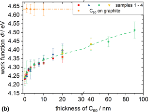
Lead-free perovskite layers may provide a good alternative to the commonly used lead-halide-based perovskite absorber layers in photovoltaics. Energy level alignment of the active semiconductor with contact layers is a key factor in device performance. Kelvin probe force microscopy was used during vapor deposition of C60 onto formamidinium tin iodide to investigate contact formation with detailed local resolution of these materials that are significant for photovoltaic cells. Significant differences dependent on the growth rate of C60 were detected. Sufficiently high deposition rates were essential to reach compact C60 films needed for good contact. A space charge layer larger than 90 nm within the C60 layer was established without indication of interfacial dipoles. The present analysis gives a clear indication of a well-functioning contact of fullerenes to formamidinium tin iodide that is suitable for the use in photovoltaic devices provided that thin compact fullerene films are formed.