Hostname: page-component-745bb68f8f-cphqk Total loading time: 0 Render date: 2025-01-09T17:37:08.608Z Has data issue: false hasContentIssue false

Comparison of convergent beam electron diffraction and annular bright field atomic imaging for GaN polarity determination

Published online by Cambridge University Press:  13 December 2016

Alexana Roshko*
Affiliation:
Applied Physics Division, NIST, Boulder, CO 80305
Matt D. Brubaker
Affiliation:
Applied Physics Division, NIST, Boulder, CO 80305
Paul T. Blanchard
Affiliation:
Applied Physics Division, NIST, Boulder, CO 80305
Kris A. Bertness
Affiliation:
Applied Physics Division, NIST, Boulder, CO 80305
Todd E. Harvey
Affiliation:
Applied Physics Division, NIST, Boulder, CO 80305
Roy H. Geiss
Affiliation:
Department of Chemistry, Colorado State University, Fort Collins, CO 80523
Igor Levin
Affiliation:
Materials Measurement Science Division, NIST, Gaithersburg, MD 20899
*
a)Address all correspondence to this author. e-mail: [email protected]
Get access

Abstract

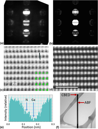
A comparison of two electron microscopy techniques used to determine the polarity of GaN nanowires is presented. The techniques are convergent beam electron diffraction (CBED) in TEM mode and annular bright field (ABF) imaging in aberration corrected STEM mode. Both measurements were made at nominally the same locations on a variety of GaN nanowires. In all cases the two techniques gave the same polarity result. An important aspect of the study was the calibration of the CBED pattern rotation relative to the TEM image. Three different microscopes were used for CBED measurements. For all three instruments there was a substantial rotation of the diffraction pattern (120 or 180°) relative to the image, which, if unaccounted for, would have resulted in incorrect polarity determination. The study also shows that structural defects such as inversion domains can be readily identified by ABF imaging, but may escape identification by CBED. The relative advantages of the two techniques are discussed.

Type
Articles
Copyright
Copyright © Materials Research Society 2016 

Access options

Get access to the full version of this content by using one of the access options below. (Log in options will check for institutional or personal access. Content may require purchase if you do not have access.)

Footnotes

Contributing Editor: Thomas Walther

References

REFERENCES

Seelmann-Eggebert, M., Weyher, J.L., Obloh, H., Zimmermann, H., Rar, A., and Porowski, S.: Polarity of (00.1) GaN epilayers grown on a (00.1) sapphire. Appl. Phys. Lett. 71(18), 26352637 (1997).CrossRefGoogle Scholar
Li, D., Sumiya, M., Yoshimura, K., Suzuki, Y., Fukuda, Y., and Fuke, S.: Characteristics of the GaN polar surface during an etching process in KOH solution. Phys. Status Solidi A 180, 357362 (2000).3.0.CO;2-F>CrossRefGoogle Scholar
Hestroffer, K., Leclere, C., Bougerol, C., Renevier, H., and Daudin, B.: Polarity of GaN nanowires grown by plasma-assisted molecular beam epitaxy on Si(111). Phys. Rev. B: Condens. Matter Mater. Phys. 84, 245302 (2011).CrossRefGoogle Scholar
Sumiya, M., Tanaka, M., Ohtsuka, K., Fuke, S., Ohnishi, T., Ohkubo, I., Yoshimoto, M., Koinuma, H., and Kawasaki, M.: Analysis of the polar direction of GaN film growth by coaxial impact collision ion scattering spectroscopy. Appl. Phys. Lett. 75, 674676 (1999).CrossRefGoogle Scholar
Auzelle, T., Haas, B., Minj, A., Bougerol, C., Rouvière, J-L., Cros, A., Colchero, J., and Daudin, B.: The influence of AlN buffer over the polarity and the nucleation of self-organized GaN nanowires. J. Appl. Phys. 117(24), 245303 (2015).CrossRefGoogle Scholar
Brubaker, M.D., Roshko, A., Blanchard, P.T., Harvey, T.E., Sanford, N.A., and Bertness, K.A.: Spontaneous growth of GaN nanowire nuclei on N- and Al-polar AlN: A piezoresponse force microscopy study of crystallographic polarity. Mater. Sci. Semicond. Process. 55(15), 6771 (2016).CrossRefGoogle Scholar
Furtmayr, F., Vielemeyer, M., Stutzmann, M., Arbiol, J., Estradé, S., Peirò, F., Morante, J.R., and Eickhoff, M.: Nucleation and growth of GaN nanorods on Si(111) surfaces by plasma-assisted molecular beam epitaxy—the influence of Si- and Mg-doping. J. Appl. Phys. 104, 034309 (2008).CrossRefGoogle Scholar
Cherns, D., Meshi, L., Griffiths, I., Khongphetsak, S., Novikov, S.V., Farley, N., Campion, R.P., and Foxon, C.T.: Defect reduction in GaN/(0001)sapphire films grown by molecular beam epitaxy using nanocolumn intermediate layers. Appl. Phys. Lett. 92, 121902 (2008).CrossRefGoogle Scholar
Chèze, C., Geelhaar, L., Brandt, O., Weber, W.M., Riechert, H., Münch, S., Rothemund, R., Reitzenstein, S., Forchel, A., Kehagias, T., Komninou, P., Dimitrakopulos, G.P., and Karakostas, T.: Direct comparison of catalyst-free and catalyst-induced GaN nanowires. Nano Res. 3, 528536 (2010).CrossRefGoogle Scholar
Brubaker, M.D., Levin, I., Davydov, A.V., Rourke, D.M., Sanford, N.A., Bright, V.M., and Bertness, K.A.: Effect of AlN buffer layer properties on the morphology and polarity of GaN nanowires grown by molecular beam epitaxy. J. Appl. Phys. 110, 053506 (2011).CrossRefGoogle Scholar
Alloing, B., Vézian, S., Tottereau, O., Vennéguès, P., Beraudo, E., and Zuniga-Péreza, J.: On the polarity of GaN micro- and nanowires epitaxially grown on sapphire (0001) and Si(111) substrates by metal organic vapor phase epitaxy and ammonia-molecular beam epitaxy. Appl. Phys. Lett. 98, 011914 (2011).CrossRefGoogle Scholar
Largeau, L., Galopin, E., Gogneau, N., Travers, L., Glas, F., and Harmand, J-C.: N-polar GaN nanowires seeded by Al droplets on Si(111). Cryst. Growth Des. 12, 27242729 (2012).CrossRefGoogle Scholar
Fernández-Garrido, S., Kong, X., Gotschke, T., Calarco, R., Geelhaar, L., Trampert, A., and Brandt, O.: Spontaneous nucleation and growth of GaN nanowires: The fundamental role of crystal polarity. Nano Lett. 12, 61196125 (2012).CrossRefGoogle ScholarPubMed
Tafto, J. and Spence, J.C.H.: A simple method for the determination of structure-factor phase relationships and crystal polarity using electron diffraction. J. Appl. Cryst. 15, 6064 (1982).CrossRefGoogle Scholar
Daudin, B., Rouviere, J.L., and Arley, M.: Polarity determination of GaN films by ion channeling and convergent beam electron diffraction. Appl. Phys. Lett. 69(17), 24802482 (1996).CrossRefGoogle Scholar
Ponce, F.A., Bour, D.P., Young, W.T., Saunders, M., and Steeds, J.W.: Determination of lattice polarity for growth of GaN bulk single crystals and epitaxial layers. Appl. Phys. Lett. 69(3), 337339 (1996).CrossRefGoogle Scholar
De Graef, M.: Introduction to Conventional Transmission Electron Microscopy, Cambridge Solid State Science Series (Cambridge University Press, Cambridge, U.K., 2003); pp. 273275.Google Scholar
Williams, D.B. and Carter, C.B.: Transmission Electron Microscopy Part 1: Basics (Springer Science+Business Media, New York, New York, 2009); pp. 167168.CrossRefGoogle Scholar
de la Mata, M., Magen, C., Gazquez, J., Utama, M.I.B., Heiss, M., Lopatin, S., Furtmayr, F., Fernández-Rojas, C.J., Peng, B., Morante, J.R., Rurali, R., Eickhoff, M., Fontcuberta i Morral, A., Xiong, Q., and Arbiol, J.: Polarity assignment in ZnTe, GaAs, ZnO, and GaN-AlN nanowires from direct dumbbell analysis. Nano Lett. 12, 25792586 (2012).CrossRefGoogle ScholarPubMed
Okunishi, E., Ishikawa, I., Sawada, H., Hosokawa, F., Hori, M., and Kondo, Y.: Visualization of light elements at ultrahigh resolution by STEM annular bright field microscopy. Microsc. Microanal. 15, 164165 (2009).CrossRefGoogle Scholar
Findlay, S.D., Shibata, N., Sawada, H., Okunishi, E., Kondo, Y., Yamamoto, T., and Ikuhara, Y.: Robust atomic resolution imaging of light elements using scanning transmission electron microscopy. Appl. Phys. Lett. 95, 191913 (2009).CrossRefGoogle Scholar
Findlay, S.D., Shibata, N., Sawada, H., Okunishi, E., Kondo, Y., and Ikuhara, Y.: Dynamics of annular bright field imaging in scanning transmission electron microscopy. Ultramicroscopy 110, 903923 (2010).CrossRefGoogle ScholarPubMed
Okunishi, E., Sawada, H., and Kondo, Y.: Experimental study of annular bright field (ABF) imaging using aberration-corrected scanning transmission electron microscopy (STEM). Micron 43, 538544 (2012).CrossRefGoogle Scholar
den Hertog, M.I., González-Posada, F., Songmuang, R., Rouviere, J.L., Fournier, T., Fernandez, B., and Monroy, E.: Correlation of polarity and crystal structure with optoelectronic and transport properties of GaN/AlN/GaN nanowire sensors. Nano Lett. 12, 56915696 (2012).CrossRefGoogle ScholarPubMed
Brubaker, M.D., Duff, S.M., Harvey, T.E., Blanchard, P.T., Roshko, A., Sanders, A.W., Sanford, N.A., and Bertness, K.A.: Polarity-controlled GaN/AlN nucleation layers for selective-area growth of GaN nanowire arrays on Si(111) substrates by molecular beam epitaxy. Cryst. Growth Des. 16, 596604 (2016).CrossRefGoogle Scholar
Zhang, X., Lourenço-Martins, H., Meuret, S., Kociak, M., Haas, B., Rouvière, J-L., Jouneau, P-H., Bougerol, C., Auzelle, T., Jalabert, D., Biquard, X., Gayral, B., and Daudin, B.: InGaN nanowires with high InN molar fraction: Growth, structural and optical properties. Nanotechnology 27, 195704 (2016).CrossRefGoogle ScholarPubMed
Aseev, P., Gačević, Ž., Torres-Pardo, A., González-Calbet, J.M., and Calleja, E.: Improving optical performance of GaN nanowires grown by selective area growth homoepitaxy: Influence of substrate and nanowire dimensions. Appl. Phys. Lett. 108, 253109 (2016).CrossRefGoogle Scholar
Phillips, P.J., Carnevale, S.D., Kumar, R., Myers, R.C., and Klie, R.F.: Full-scale characterization of UVLED Al x Ga1−x N nanowires via advanced electron microscopy. ACS Nano 7, 50455051 (2013).CrossRefGoogle Scholar
Bertness, K.A., Roshko, A., Mansfield, L.M., Harvey, T.E., and Sanford, N.A.: Mechanism for spontaneous growth of GaN nanowires with molecular beam epitaxy. J. Cryst. Growth. 310, 31543158 (2008).CrossRefGoogle Scholar
Disclaimer: Commercial instruments are identified only in order to adequately specify certain procedures. In no case does such identification imply recommendation or endorsement by the National Institute of Standards and Technology, nor does it imply that the products identified are necessarily the best available for the purpose.Google Scholar
Mitate, T., Mizuno, S., Takahata, H., Kakegawa, R., Matsuokab, T., and Kuwano, N.: InN polarity determination by convergent-beam electron diffraction. Appl. Phys. Lett. 86, 134103 (2005).CrossRefGoogle Scholar
Liu, F., Collazo, R., Mita, S., Sitar, Z., Pennycook, S.J., and Duscher, G.: Direct observation of inversion domain boundaries of GaN on c-sapphire at Sub-Ångstrom resolution. Adv. Mater. 10, 21622165 (2008).CrossRefGoogle Scholar
Stadelmann, P.A.: EMS—A software package for electron diffraction analysis and HREM image simulation in materials science. Ultramicroscopy 21, 131145 (1987).CrossRefGoogle Scholar
Urban, A., Malindretos, J., Klein-Wiele, J-H., Simon, P., and Rizzi, A.: Ga-polar GaN nanocolumn arrays with semipolar faceted tips. New J. Phys. 15, 053045 (2013).CrossRefGoogle Scholar
Gačević, Ž., Bengoechea-Encabo, A., Albert, S., Torres-Pardo, A., González-Calbet, J.M., and Calleja, E.: Crystallographically uniform arrays of ordered (In)GaN nanocolumns. J. Appl. Phys. 117, 035301 (2015).CrossRefGoogle Scholar
Zuo, J.M.: Convergent beam electron diffraction. In Electron Crystallography, Weirich, T.E., Lábár, J.L., and Zou, X. eds.; Springer NATO Science Series: Dordrecht, The Netherlands, 2006; pp. 143168.CrossRefGoogle Scholar
Howie, A.: Quantitative experimental study of dislocations and stacking faults by transmission electron microscopy. Metall. Rev. 6, 467503 (1961).CrossRefGoogle Scholar