Hostname: page-component-cd9895bd7-gvvz8 Total loading time: 0 Render date: 2024-12-18T14:43:21.107Z Has data issue: false hasContentIssue false

Band gap-tuned MoS2(1−x)Te2x thin films synthesized by a hybrid Co-sputtering and post-deposition tellurization annealing process

Published online by Cambridge University Press:  10 August 2017

Yusuke Hibino*
Affiliation:
School of Science and Technology, Meiji University, Kawasaki-shi, Kanagawa-ken 214-8571, Japan
Seiya Ishihara
Affiliation:
School of Science and Technology, Meiji University, Kawasaki-shi, Kanagawa-ken 214-8571, Japan
Naomi Sawamoto
Affiliation:
School of Science and Technology, Meiji University, Kawasaki-shi, Kanagawa-ken 214-8571, Japan
Takumi Ohashi
Affiliation:
School of Engineering Department of Electrical and Electronic Engineering, Tokyo Institute of Technology, Yokohama-shi, Kanagawa-ken 226-8502, Japan
Kentarou Matsuura
Affiliation:
School of Engineering Department of Electrical and Electronic Engineering, Tokyo Institute of Technology, Yokohama-shi, Kanagawa-ken 226-8502, Japan
Hideaki Machida
Affiliation:
Gas-Phase Growth Ltd., Tokyo University of Agriculture and Technology, Koganei-shi, Tokyo-to 184-0012, Japan
Hitoshi Wakabayashi
Affiliation:
School of Engineering Department of Electrical and Electronic Engineering, Tokyo Institute of Technology, Yokohama-shi, Kanagawa-ken 226-8502, Japan
Atsushi Ogura
Affiliation:
School of Science and Technology, Meiji University, Kawasaki-shi, Kanagawa-ken 214-8571, Japan
*
a) Address all correspondence to this author. e-mail: [email protected]
Get access

Abstract

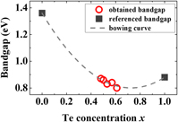
MoS2(1−x)Te2x thin films were fabricated by high-temperature co-sputtering deposition and post-deposition tellurization annealing using novel Te precursor (i-C3H7)2Te for the first time. As a result, high crystal quality MoS2(1−x)Te2x (6.5 nm) were successfully fabricated with the Te concentration x ranging from 0.48 to 0.61 and band gap value from 0.80 to 0.87 eV. From the obtained band gap values of MoS2(1−x)Te2x , the bowing parameter b was determined to be 1.06 eV. When exploited in device use, if the required band gap value is known, the required composition can be calculated with the bowing parameter. We have also shown the compatibility of co-sputtering to alloy fabrication since the composition ratio can be easily controlled just by adjusting the radio frequency (RF) sputter power on different targets. The fabrication method can be applied to different transition metal dichalcogenide materials as well.

Type
Invited Paper
Copyright
Copyright © Materials Research Society 2017 

Access options

Get access to the full version of this content by using one of the access options below. (Log in options will check for institutional or personal access. Content may require purchase if you do not have access.)

Footnotes

Contributing Editor: Gary L. Messing

References

REFERENCES

Xu, M.S., Liang, T., Shi, M., and Chen, H.Z.: Graphene-like two-dimensional materials. Chem. Rev. 113, 3766 (2013).CrossRefGoogle ScholarPubMed
Zhang, W., Huang, Z., Zhang, W., and Li, Y.: Two-dimensional semiconductors with possible high room temperature mobility. Nano Res. 7, 1731 (2014).Google Scholar
Komsa, H.P. and Krasheninnikov, A.V.: Two-dimensional transition metal dichalcogenide alloys: Stability and electronic properties. J. Phys. Chem. Lett. 3, 3652 (2012).Google Scholar
Chen, Y., Xi, J., Dumcenco, D.O., Liu, Z., Suenaga, K., Wang, D., Shuai, Z., Huang, Y.S., and Xie, L.: Tunable band gap photoluminescence from atomically thin transition-metal dichalcogenide alloys. ACS Nano 7, 4610 (2013).Google Scholar
Dumcenco, D.O., Kobayashi, H., Liu, Z., Huang, Y.S., and Suenaga, K.: Visualization and quantification of transition metal atomic mixing in Mo1−x W x S2 single layers. Nat. Commun. 4, 1351 (2013).Google Scholar
Dumcenco, D.O., Chen, K.Y., Wang, Y.P., Huang, Y.S., and Tiong, K.K.: Raman study of 2H–Mo1−x W x S2 layered mixed crystals. J. Alloys Compd. 506, 940 (2010).CrossRefGoogle Scholar
Liu, H., Antwi, K.K.A., Chua, S., and Chi, D.: Vapor-phase growth and characterization of Mo1−x W x S2 (0 ≤ x ≤ 1) atomic layers on 2-inch sapphire substrates. Nanoscale 6, 624 (2014).Google Scholar
Yina, G.L., Huanga, P.H., Yua, Z., Hea, D.N., and Tub, J.P.: Microstructure, chemical and tribological investigations of Mo x W1−x S y co-sputtered composite films. Tribol. Lett. 22, 37 (2006).CrossRefGoogle Scholar
Mann, J., Ma, Q., Odenthal, P.M., Isarraraz, M., Le, D., Preciado, E., Barroso, D., Yamaguchi, K., von Son Palacio, G., Nguyen, A., Tran, T., Wurch, M., Nguyen, A., Klee, V., Bobek, S., Sun, D., Heinz, T.F., Rahman, T.S., Kawakami, R., and Bartels, L.: 2-Dimensional transition metal dichalcogenides with tunable direct band gaps: MoS2(1–x)Se2x monolayers. Adv. Mater. 26, 1399 (2014).CrossRefGoogle Scholar
Muratore, C., Hu, J.J., Wang, B., Haque, M.A., Bultman, J.E., Jespersen, M.L., Shamberger, P.J., McConney, M.E., Naguy, R.D., and Voevodin, A.A.: Continuous ultra-thin MoS2 films grown by low-temperature physical vapor deposition. Appl. Phys. Lett. 104, 261604 (2014).Google Scholar
Ishihara, S., Hibino, Y., Sawamoto, N., Suda, K., Ohashi, T., Matsuura, K., Machida, H., Ishikawa, M., Sudoh, H., Wakabayashi, H., and Ogura, A.: Improving crystalline quality of sputtering-deposited MoS2 thin film by postdeposition sulfurization annealing using (t-C4H9)2S2 . Jpn. J. Appl. Phys. 55, 04EJ07 (2016).Google Scholar
Ruppert, C., Aslan, O.B., and Heinz, T.F.: Optical properties and band gap of single- and few-layer MoTe2 crystals. Nano Lett. 14, 6231 (2014).CrossRefGoogle ScholarPubMed
Lezama, I.G., Ubaldini, A., Longobardi, M., Giannini, E., Renner, C., Kuzmenko, A.B., and Morpurgo, A.F.: Surface transport and band gap structure of exfoliated 2H–MoTe2 crystals. 2D Mater. 1, 2 (2014).Google Scholar
Radisavljevic, B., Radenovic, A., Brivio, J., Giacometti, V., and Kis, A.: Single-layer MoS2 transistors. Nat. Nanotechnol. 6, 147 (2011).CrossRefGoogle ScholarPubMed
Das, S., Demarteau, M., and Roelofs, A.: Nb-doped single crystalline MoS2 field effect transistor. Appl. Phys. Lett. 106, 173506 (2015).CrossRefGoogle Scholar
Yoon, Y., Ganapathi, K., and Salahuddin, S.: How good can monolayer MoS2 transistors Be? Nano Lett. 11, 3768 (2011).CrossRefGoogle Scholar
Pradhan, N.R., Rhodes, D., Feng, S., Xin, Y., Memaran, S., Moon, B-H., Terrones, H., Terrones, M., and Balicas, L.: Field-effect transistors based on few-layered α-MoTe2 . ACS Nano 8, 5911 (2014).Google Scholar
Zheng, Z.Q., Zhang, T.M., Yao, J.D., Zhang, Y., Xu, J.R., and Yang, G.W.: Flexible, transparent and ultra-broadband photodetector based on large-area WSe2 film for wearable devices. Nanotechnology 27, 225501 (2016).Google Scholar
Zheng, Z.Q., Yao, J.D., and Yang, G.W.: Growth of centimeter-scale high-quality In2Se3 films for transparent, flexible and high performance photodetectors. J. Mater. Chem. C 4, 8094 (2016).CrossRefGoogle Scholar
Samnakay, R., Jiang, C., Rumyantsev, S.L., Shur, M.S., and Balandin, A.A.: Selective chemical vapor sensing with few-layer MoS2 thin-film transistors: Comparison with graphene devices. Appl. Phys. Lett. 106, 023115 (2015).Google Scholar
Ozaki, K., Kiyama, T., Hirahara, K., Tanaka, N., Kuwabata, S., and Torimoto, T.: Single-step synthesis of gold–silver alloy nanoparticles in ionic liquids by a sputter deposition technique. Chem. Commun. 6, 691 (2008).Google Scholar
Ho, K.K. and Carman, G.P.: Sputter deposition of NiTi thin film shape memory alloy using a heated target. Thin Solid Films 370, 18 (2000).CrossRefGoogle Scholar
Sato, H., Shimatsu, T., Okazaki, Y., Muraoka, H., and Aoi, H.: Fabrication of L11 type Co–Pt ordered alloy films by sputter deposition. J. Appl. Phys. 103, 07E114 (2016).Google Scholar
Ishihara, S., Hibino, Y., Sawamoto, N., Ohashi, T., Matsuura, K., Machida, H., Ishikawa, M., Wakabayashi, H., and Ogura, A.: Large scale uniformity of sputtering deposited single- and few-layer MoS2 investigated by XPS multipoint measurements and histogram analysis of optical contrast. ECS J. Solid State Sci. Technol. 5, Q3012 (2016).Google Scholar
Ohashi, T., Suda, K., Ishihara, S., Sawamoto, N., Yamaguchi, S., Matsuura, K., Kakushima, K., Sugii, N., Nishiyama, A., Kataoka, Y., Natori, K., Tsutsui, K., Iwai, H., Ogura, A., and Wakabayashi, H.: Multi-layered MoS2 film formed by high-temperature sputtering for enhancement-mode nMOSFETs. Jpn. J. Appl. Phys. 54, 04DN08 (2015).Google Scholar
Kamiya, T., Nomura, K., and Hosono, H.: Electronic structure of the amorphous oxide semiconductor a-InGaZnO4–x : Tauc–Lorentz optical model and origins of subgap states. Phys. Status Solidi A 206, 860 (2009).Google Scholar
Shaaban, E.R., Abd El-Sadek, M.S., El-Hagary, M., and Yahia, I.S.: Spectroscopic ellipsometry investigations of the optical constants of nanocrystalline SnS thin films. Phys. Scr. 86, 015702 (2012).Google Scholar
Wang, Z., Wang, W., Yang, Y., Li, W., Feng, L., Zhang, J., Wu, L., and Zeng, G.: The structure and stability of molybdenum ditelluride thin films. Int. J. Photoenergy, 28, 956083 (2014).Google Scholar
Moser, J. and Lévy, F.: Growth mechanism and near-interface structure in relation to orientation of MoS2 sputtered thin films. J. Mater. Res. 7, 734 (1992).Google Scholar
Liu, D., Guo, Y., Fang, L., and Robertson, J.: Sulfur vacancies in monolayer MoS2 and its electrical contacts. Appl. Phys. Lett. 103, 183113 (2013).Google Scholar
Ishihara, S., Suda, K., Hibino, Y., Sawamoto, N., Ohashi, T., Yamaguchi, S., Matsuura, K., Machida, H., Ishikawa, M., Sudoh, H., Wakabayashi, H., and Ogura, A.: Evaluation of sputtering deposited 2-dimensional MoS2 film by Raman spectroscopy. MRS Proc. 1781, 11 (2015).CrossRefGoogle Scholar
Ishihara, S., Hibino, Y., Sawamoto, N., Suda, K., Ohashi, T., Matsuura, K., Machida, H., Ishikawa, M., Sudoh, H., Wakabayashi, H., and Ogura, A.: Properties of single-layer MoS2 film fabricated by combination of sputtering deposition and post deposition sulfurization annealing using (t-C4H9)2S2 . Jpn. J. Appl. Phys. 55, 06GF01 (2016).Google Scholar
Bernèdea, J.C., Amorya, C., Assmanna, L., and Spiesserb, M.: X-ray photoelectron spectroscopy study of MoTe2 single crystals and thin films. Appl. Surf. Sci. 219, 238 (2003).Google Scholar
Firefly version 8. Available at: http://classic.chem.msu.su/gran/firefly/index.html (accessed May 28, 2016).Google Scholar
Schmidt, M.W., Baldridge, K.K., Boatz, J.A., Elbert, S.T., Gordon, M.S., Jensen, J.H., Koseki, S., Matsunaga, N., Nguyen, K.A., Su, S., Windus, T.L., Dupuis, M., and Montgomery, J.A.: General atomic and molecular electronic structure system. J. Comput. Chem. 14, 1347 (1993).CrossRefGoogle Scholar