Hostname: page-component-745bb68f8f-kw2vx Total loading time: 0 Render date: 2025-01-07T18:03:41.439Z Has data issue: false hasContentIssue false

Novel nanosample preparation with a helium ion microscope

Published online by Cambridge University Press:  03 April 2013

Maria Rudneva*
Affiliation:
Delft University of Technology, Kavli Institute of Nanoscience, 2628 CJ Delft, The Netherlands
Emile van Veldhoven
Affiliation:
TNO - van Leeuwenhoek Laboratory, 2826 CK Delft, The Netherlands
Sairam K. Malladi
Affiliation:
Delft University of Technology, Kavli Institute of Nanoscience, 2628 CJ Delft, The Netherlands
Diederik Maas
Affiliation:
TNO - van Leeuwenhoek Laboratory, 2826 CK Delft, The Netherlands
Henny W. Zandbergen
Affiliation:
Delft University of Technology, Kavli Institute of Nanoscience, 2628 CJ Delft, The Netherlands
*
a)Address all correspondence to this author. e-mail: [email protected]
Get access

Abstract

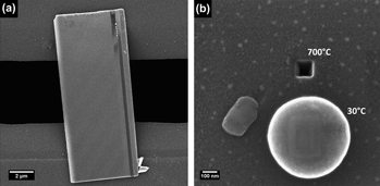
In this article, we present novel sample preparation methods using a helium ion microscope (HIM). We report the possibility of reshaping, at room temperature, thin metal lines on an electron-transparent membrane: A set of platinum bridges with standard geometry (300 × 200 × 15 nm) was modified at room temperature into different shapes using focused helium (He)-ion beam. Also the applicability of the HIM as a tool for precise modification of silicon (Si) and strontium titanate (SrTiO3) lamellae is shown and discussed. We demonstrated that in situ heating (e.g., at 600 °C) of the samples during He-beam illumination by use of a specially developed heating stage enables production of thin Si and SrTiO3 samples without significant artifacts. The quality of such cuts was inspected by transmission electron microscopy with high-resolution imaging, and the diffraction patterns were analyzed.

Type
Invited Feature Papers
Copyright
Copyright © Materials Research Society 2013

Access options

Get access to the full version of this content by using one of the access options below. (Log in options will check for institutional or personal access. Content may require purchase if you do not have access.)

References

REFERENCES

Livengood, R.: Subsurface damage from helium ions as a function of dose, beam energy, and dose rate. J. Vac. Sci. Technol., B 27(6), 32443249 (2009).Google Scholar
Raineri, V. and Saggio, M.: Radiation damage and implanted He atoms interaction during void formation in silicon. Appl. Phys. Lett. 71, 12 (1997).CrossRefGoogle Scholar
Ziegler, J.F., Biersack, J.P., and Ziegler, M.D.: SRIM - The Stopping and Range of Ions in Matter (SRIM Co., Chester, MD, 2008). Srim Co.,ISBN 9780965420716.Google Scholar
Maas, D.J., van der Drift, E.W., van Veldhoven, E., Meessen, J., Rudneva, M., and Alkemade, P.F.A.: Nano-engineering with a focused helium ion beam, in Ion Beams–New Applications from Mesoscale to Nanoscale, edited by Baglin, J., Ila, D., Marletta, G., and Ӧztarhan, A. (Mater. Res. Soc.Symp. Proc. 1354, Warrendale, PA, 2011), p. 33.Google Scholar
Alkemade, P.F., Koster, E.M., van Veldhoven, E., and Maas, D.J.: Imaging and nanofacrication with the helium ion microscope of the Van Leeuwenhoek Laboratory in Delft. Scanning 34(2), 90100 (2012).Google Scholar
Ward, B.W., Notte, J.A., and Economou, N.P.: Helium ion microscope: A new tool for nanoscale microscopy and metrology. J. Vac. Sci. Technol., B 24(6), 28712874 (2006).CrossRefGoogle Scholar
Bell, D.C.: Contrast mechanisms and image formation in helium ion microscope. Microsc. Microanal. 15(2), 147153 (2009).CrossRefGoogle Scholar
Postek, M.T., Vladar, A., Archie, C., and Ming, B.: Review of current progress in nanometrology with the helium ion microscope. Meas. Sci. Technol. 22, 2 (2011).Google Scholar
Sidorkin, V., van Veldhoven, E., van der Drift, E.W., Alkemade, P.F., Salemnik, H., and Maas, D.: Sub-10-nm nanolithography with a scanning helium beam. J. Vac. Sci. Technol., B 27(4), L18L20 (2009).Google Scholar
Winston, D., Cord, B.M., Ming, B., Bell, D.C., DiNatale, W.F., Stern, L.A., Vladar, A.E., Postek, M.T., Mondol, M.K., Yang, J.K.W., and Berggren, K.K.: Scanning-helium-ion-beam lithography with hydrogen silsesquioxane resist. J. Vac. Sci. Technol., B 27(6), 27022706 (2009).Google Scholar
Maas, D., van Veldhoven, E., Chen, P., Sidorkin, V., Salemink, H., van der Drift, E., and Alkemade, P.: Nanofabrication with a helium ion microscope. In SPIE Metrology, Inspection, and Process Control for Microlithography XXIV, 7638, edited by C.J. Raymond (SPIE Press, Bellingham, WA, 2010), p. 763814.Google Scholar
Drezner, Y., Greenzweig, Y., Fishman, D., van Veldhoven, E., Maas, D.J., Raveh, A., and Livengood, R.H.: Structural characterization of He ion microscope platinum deposition and sub-surface silicon damage. J. Vac. Sci. Technol., B 30, 4 (2012).CrossRefGoogle Scholar
Lemme, M.C., Bell, D.C.. Williams, J.R., Stern, L.A., Baugher, B.W.H., Jarillo-Herrero, P., and Marcus, C.M.: Etching of graphene devices with a helium ion beam. ACS Nano 3(9), 26742676 (2009).Google Scholar
Yang, J., Ferranti, D.C., Stern, L.A., Sanford, C.A., Huang, J., Ren, Z., Qin, L-C., and Hall, A.R.: Rapid and precise scanning helium ion microscope milling of solid-state nanopores for biomolecule detection. Nanotechnology 22, 285310 (2011).Google Scholar
van Huis, M.A., Young, N.P., Pandraud, G., Creemer, J.F., Vanmaekelbergh, D., Kirkland, A.I., and Zandbergen, H.W.: Atomic imaging of phase transitions and morphology transformation in nanocrystals. Adv. Mater. 21, 49924995 (2009).Google Scholar
Rue, C., Shepherd, R., Hallstein, R., and Livengood, R.: Low keV FIB Applications for Circuit Edit. ISTFA2007, San Jose, CA (ASM International, Novelty, OH, 2007), pp. 312318.Google Scholar
da Silva, D., Morschbacher, M.J., Fichtner, P.F.P., Oliviero, E., and Behar, M.: Formation of bubbles and extended defects in He implanted (1 0 0) Si at elevated temperatures. Nucl. Instrum. Methods Phys. Res., Sect. B 219220, 713717 (2004).Google Scholar
David, M.L., Beaufort, M.F., and Barbot, J.F.: Effect of implant temperature on defects created using high fluence of helium in silicon. J. Appl. Phys. 93(3), 1438 (2003).Google Scholar
Jia, C.L., Thust, A., and Urban, L.: Atomic-scale analysis of the oxygen configuration at SrTiO3. Phys. Rev. Lett. 95(22), 225506 (2005).Google Scholar
Szot, K., Speier, W., Carius, R., Zastrow, U., and Beyer, W.: Localized metallic conductivity and self-healing during thermal reduction of SrTiO3. Phys. Rev. Lett. 88, 075508 (2002).Google Scholar
Haeni, J.H., Irvin, P., Chang, W., Uecker, R., Reiche, P., Li, Y.L., Choudhury, S., Tian, W., Hawley, M.E., Craigo, B., Tagantsev, A.K., Pan, X.Q., Streiffer, S.K., Chen, L.Q., Kirchoefer, S.W., Levy, J., and Schlom, D.G.: Room-temperature ferroelectricity in strained SrTiO3. Nature 430, 758 (2004).CrossRefGoogle ScholarPubMed
Rudneva, M., Gao, B., Prins, F., Xu, Q., van der Zant, H.S.J., and Zandbergen, H.W.: In situ transmission electron microscopy imaging of electromigration in Pt nanowires. Microsc. Microanalysis (2012).Google Scholar
Gao, B., Rudneva, M., McGarrity, K.S., Xu, Q., Prins, F., Thijssen, J.M., Zandbergen, H., and van der Zant, H.S.J.: In situ transmission electron microscopy imaging of grain growth in a platinum nanobridge induced by electric current annealing. Nanotechnology 22, 205705 (2011).Google Scholar
Rudneva, M., van Veldhoven, E., Maas, D., and Zandbergen, H.W.: Helium Ion Microscope as a Sculpting Tool for Nanoscamples (Proceedings of International Union of Microbeam Analysis Societies –V, Seoul, South Korea, 2011).Google Scholar
Reutov, V.F. and Sokhatskii, A.S.: Formation of ordered helium pores in amorphous silicon subjected to low-energy helium ion irradiation. Tech. Phys. 48(1), 7378 (2003).Google Scholar
Jung, P.: Diffusion of implanted helium in Si and SiO2. Nucl. Instrum. Methods Phys. Res. Sect., B 91(1–4), 362365 (1994).Google Scholar