Hostname: page-component-586b7cd67f-2plfb Total loading time: 0 Render date: 2024-11-28T17:28:19.782Z Has data issue: false hasContentIssue false

Localized recrystallization and cracking of lead-free solder interconnections under thermal cycling

Published online by Cambridge University Press:  16 August 2011

Hongtao Chen
Affiliation:
Department of Electronic, Aalto University School of Science and Technology, FIN-00076 Aalto, Finland; and Shenzhen Graduate School, Harbin Institute of Technology, Shenzhen 518055, China
Maik Mueller
Affiliation:
Electronics Packaging Laboratory (IAVT), Technische Universität Dresden, 01062 Dresden, Germany
Tonu Tuomas Mattila*
Affiliation:
Department of Electronic, Aalto University School of Science and Technology, FIN-00076 Aalto, Finland
Jue Li
Affiliation:
Department of Electronic, Aalto University School of Science and Technology, FIN-00076 Aalto, Finland
Xuwen Liu
Affiliation:
Laboratory of Materials Science, Department of Materials Science and Engineering, Aalto University School of Chemical Technology, FIN-00076 Aalto, Finland
Klaus-Juergen Wolter
Affiliation:
Electronics Packaging Laboratory (IAVT), Technische Universität Dresden, 01062 Dresden, Germany
Mervi Paulasto-Kröckel
Affiliation:
Department of Electronic, Aalto University School of Science and Technology, FIN-00076 Aalto, Finland
*
a)Address all correspondence to this author. e-mail: [email protected]
Get access

Abstract

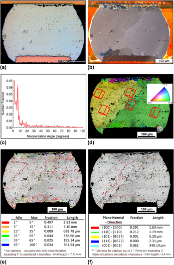
The failure mechanism of lead-free solder interconnections of chip scale package–sized Ball Grid Array (BGA) component boards under thermal cycling was studied by employing cross-polarized light microscopy, scanning electronic microscopy, electron backscatter diffraction, and nanoindentation. It was determined that the critical solder interconnections were located underneath the chip corners, instead of the corner most interconnections of the package, and the highest strains and stresses were concentrated at the outer neck regions on the component side of the interconnections. Observations of the failure modes were in good agreement with the finite element results. The failure of the interconnections was associated with changes of microstructures by recrystallization in the strain concentration regions of the solder interconnections. Coarsening of intermetallic particles and the disappearance of the boundaries between the primary Sn cells were observed in both cases. The nanoindentation results showed lower hardness of the recrystallized grains compared with the non-recrystallized regions of the same interconnection. The results show that failure modes are dependent on the localized microstructural changes in the strain concentration regions of the interconnections and the crack paths follow the networks of grain boundaries produced by recrystallization.

Type
Articles
Copyright
Copyright © Materials Research Society 2011

Access options

Get access to the full version of this content by using one of the access options below. (Log in options will check for institutional or personal access. Content may require purchase if you do not have access.)

References

REFERENCES

1.Zeng, K. and Tu, K.N.: Six cases of reliability study of Pb-free solder joints in electronic packaging technology. Mater. Sci. Eng., R 38, 55 (2002).CrossRefGoogle Scholar
2.Shang, J.K., Zeng, Q.L., Zhang, L., and Zhu, Q.S.: Mechanical fatigue of Sn-rich Pb-free solder alloys. J. Mater. Sci.- Mater. Electron. 18, 211 (2007).CrossRefGoogle Scholar
3.Kim, J.W., Kim, D.G., Hong, W.S., and Jung, S.B.: Evaluation of solder joint reliability in flip-chip packages during accelerated testing. J. Electron. Mater. 34, 1550 (2005).CrossRefGoogle Scholar
4.Erinç, M., Schreurs, P.J.G., Zhang, G.Q., and Geers, M.G.D.: Microstructural damage analysis of SnAgCu solder joints and an assessment on indentation procedures. J. Mater. Sci.- Mater. Electron. 16, 693 (2005).CrossRefGoogle Scholar
5.Chiang, H.W., Chen, J.Y., Chen, M.C., Lee, J.C.B., and Shiau, G.: Reliability testing of WLCSP lead-free solder joints. J. Electron. Mater. 35, 1032 (2006).CrossRefGoogle Scholar
6.Lee, W.W., Nguyen, L.T., and Selvaduray, G.S.: Solder joint fatigue models: Review and applicability to chip scale packages. Microelectron. Reliab. 40, 231 (2000).CrossRefGoogle Scholar
7.Mattila, T.T., Vuorinen, V., and Kivilahti, J.K.: Impact of printed wiring board coatings on the reliability of lead-free chip-scale package interconnections. J. Mater. Res. 19, 3214 (2004).CrossRefGoogle Scholar
8.Terashima, S. and Tanaka, M.: Thermal fatigue properties of Sn–1.2Ag–0.5Cu–xNi flip chip interconnects. Mater. Trans. 45, 681 (2004).CrossRefGoogle Scholar
9.Henderson, D.W., Woods, J.J., Gosselin, T.A., Bartelo, J., King, D.E., Korhonen, T.M., Korhonen, M.A., Lehman, L.P., Cotts, E.J., Kang, S.K., Lauro, P., Shih, D.Y., Goldsmith, C., and Puttlitz, K.J.: The microstructure of Sn in near-eutectic Sn-Ag-Cu alloy solder joints and its role in thermomechanical fatigue. J. Mater. Res. 19, 1608 (2004).CrossRefGoogle Scholar
10.Telang, A.U., Bieler, T.R., Zamiri, A., and Pourboghrat, F.: Incremental recrystallization/grain growth driven by elastic strain energy release in a thermomechanically fatigued lead-free solder joint. Acta Mater. 55, 2265 (2007).CrossRefGoogle Scholar
11.Sundelin, J.J., Nurimi, S.T., and Lepistö, T.K.: Recrystallization behavior of SnAgCu solder joints. Mater. Sci. Eng., A 474, 201 (2008).CrossRefGoogle Scholar
12.Hardwick, D., Sellars, C.M., and Tegart, W.J.McG.: The occurrence of recrystallization during high-temperature creep. J. Inst. Met. 90, 21 (1961).Google Scholar
13.McLean, D. and Farmer, M.H.: The relation during creep between grain–boundary sliding, sub–crystal size, and extension. J. Inst. Met. 85, 41 (1956).Google Scholar
14.Miettinen, S.: Recrystallization of lead-free solder joints under mechanical load, Master's Thesis (Helsinki University of Technology, Espoo, Finland, 2005).Google Scholar
15.Mattila, T.T., Laurila, T., and Kivilahti, J.K.: Metallurgical factors behind the reliability of high density lead-free interconnections, in Micro- and Opto-electronic Materials and Structures: Physics, Mechanics, Design, Reliability, Packaging, Vol. 1, edited by Suhir, E., Wong, C. P., and Lee, Y. C. (Springer, New York, 2007), pp. 313350.Google Scholar
16.Terashima, S., Takahama, K., Nozaki, M., and Tanaka, M.: Recrystallization of Sn grains due to thermal strain in Sn-1.2Ag-0.5Cu-0.05Ni solder. Mater. Trans. 45, 1383 (2004).CrossRefGoogle Scholar
17.Vianco, P.T., Rejent, J.A., and Kilgo, A.C.: Time-independent mechanical and physical properties of the ternary 95.5Sn–3.9Ag–0.6Cu solder. J. Electron. Mater. 32, 142 (2003).CrossRefGoogle Scholar
18.Lauro, P., Kang, S.K., Choi, W.K., and Shih, D-Y.: Effect of mechanical deformation and annealing on the microstructure and hardness of Pb-free solders. J. Electron. Mater. 32, 1432 (2003).CrossRefGoogle Scholar
19.Karppinen, J.: A comparative study of power cycling and thermal shock tests, in Proceedings of the First Electronics System-Integration Technology Conference, 2006, pp. 187194.Google Scholar
20.Nurminen, K.: Reliability of lead-free solder interconnections in thermal shock and power cycling tests, Master’s Thesis, Espoo, 2006.Google Scholar
21.Mattila, T.T. and Kivilahti, J.K.: The role of recrystallization in the failure mechanism of SnAgCu solder interconnections under thermomechanical loading. IEEE Trans. Compon. Packag. Technol. 33, 629 (2010).CrossRefGoogle Scholar
22.Metals Handbook: Vol. 2. Properties and Selection: Nonferrous Alloys and Special-Purpose Materials, 10th ed.ASM International Handbook Committee (ASM International, 1990).Google Scholar
23.MatWeb Material Property Data (Online). Available athttp://www.matweb.com (referenced January 22, 2008).Google Scholar
24.Coombs, C.F. Jr.: Printed Circuits Handbook, 5th ed. (McGraw–Hill, New York, 2001).Google Scholar
25.Anand, L.: Constitutive equations for rate-dependent deformation of metals at elevated temperatures. J. Eng. Mater. Technol. ASME 104, 12 (1982).CrossRefGoogle Scholar
26.Reinikainen, T.O., Marjamäki, P., and Kivilahti, J.K.: Deformation characteristics and microstructural evolution of SnAgCu solder interconnections, in Proceedings of the Sixth International Conference on Thermal, Mechanical, Multiphysics Simulation and Experiments in Micro-electronics and Micro-systems, EuroSimE, 2005, pp. 9198.Google Scholar
27.Dudek, R., Faust, W., Ratchev, R., Roellig, M., Albrecht, H-J., and Michel, B.: Thermal test- and field cycling induced degradation and its FE-based prediction for different SAC solders, in 11th Intersociety Conference on Thermal and Thermomechanical Phenomena in Electronic Systems (ITHERM), 2008, pp. 668675.Google Scholar
28.Moon, K.W., Boettinger, W.J., Kattner, U.R., Biancaniello, F.S., and Handwerker, C.A.: Experimental and thermodynamic assessment of Sn-Ag-Cu solder alloys. J. Electron. Mater. 29, 1122 (2000).CrossRefGoogle Scholar
29.Terashima, S., Kohno, T., Mizusawa, A., AraiI, K., Okada, O., Wakabayash, T., Tanaka, M., and Tatsumi, K.: Improvement of thermal fatigue properties of Sn-Ag-Cu lead-free solder interconnects on Casio’s wafer-level packages based on morphology and grain boundary character. J. Electron. Mater. 38, 33 (2009).CrossRefGoogle Scholar
30.Terashima, S. and Tanaka, M.: Effect of fine dispersoids and anisotropic nature of β-Sn on thermal fatigue properties of flip chips connected by Sn-xAg-0·5Cu (x: 1, 3 and 4 mass-%) lead free solders. Sci. Technol. Weld. Joining 14, 468 (2009).CrossRefGoogle Scholar
31.Panchenko, I., Mueller, M., Wiese, S., Schindler, S., and Wolter, K-J.: Solidification processes in the Sn-rich part of the SnCu system, The Proceedings of the 61st Electronic Components and Technology Conference, 2011, pp. 9099.Google Scholar
32.Seo, S-K., Kang, S.K., Cho, M.G., Shih, S-Y., and Lee, H.M.: The crystal orientation of β-Sn grains in Sn-Ag and Sn-Cu solders affected by their interfacial reactions with Cu and Ni(P) under bump metallurgy. J. Electron. Mater. 38, 2461 (2009).CrossRefGoogle Scholar
33.Bader, W.G.: Dissolution of Au, Ag, Pd, Pt, Cu and Ni in a molten tin-lead solder. Weld. J. 48, 551 (1969).Google Scholar
34.Lehman, L.P., Xing, Y., Bieler, T.R., and Cotts, E.J.: Cyclic twin nucleation in tin-based solder alloys. Acta Mater. 58, 3546 (2010).CrossRefGoogle Scholar
35.Zhou, B., Bieler, T.T., Lee, T.K., and Liu, K.C.: Crack development in a low-stress PBGA package due to continuous recrystallization leading to formation of orientations with [001] parallel to the interface. J. Electron. Mater. 39, 2669 (2010).CrossRefGoogle Scholar
36.Vianco, P.T., Rejent, J.A., and Kilgo, A.C.: Creep behavior of the ternary 95.5Sn-3.9Ag-0.6Cu solder—Part I: As-cast condition. J. Electron. Mater. 33, 1389 (2004).CrossRefGoogle Scholar
37.Dutta, I.: A constitutive model for creep of lead-free solders undergoing strain-enhanced microstructural coarsening: A first report. J. Electron. Mater. 32, 201 (2003).CrossRefGoogle Scholar
38.Dutta, I., Kumar, P., and Subbarayan, G.: Microstructural coarsening in Sn-Ag-based solders and its effects on mechanical properties. JOM 61, 29 (2009).CrossRefGoogle Scholar
39.Pearson, W.B.: A Handbook of Lattice Spacings and Structure of Metals and Alloys, Vol. 2 (Pergamon Press, London, 1958).Google Scholar