Hostname: page-component-586b7cd67f-vdxz6 Total loading time: 0 Render date: 2024-11-24T14:49:49.109Z Has data issue: false hasContentIssue false

Electron transport properties of graphene with charged impurities and vacancy defects

Published online by Cambridge University Press:  26 March 2013
Yasuhiko Kudo*
Affiliation:
Department of Chemistry, Graduate School of Science and Engineering, Tokyo Institute of Technology, Meguro-ku, Tokyo 152-8551, Japan
Kazuyuki Takai*
Affiliation:
Department of Chemistry, Graduate School of Science and Engineering, Tokyo Institute of Technology, Meguro-ku, Tokyo 152-8551, Japan
Toshiaki Enoki*
Affiliation:
Department of Chemistry, Graduate School of Science and Engineering, Tokyo Institute of Technology, Meguro-ku, Tokyo 152-8551, Japan
*
a)Address all correspondence to these authors. e-mail: [email protected]
Get access

Abstract

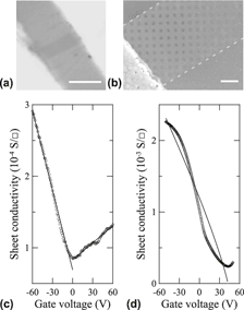
Nano-structured graphene has recently attracted extraordinary attention due to its potential use as an electronic or spintronic material. We investigated the electrical conductivities of antidot and Ar-sputtered graphene samples under a magnetic field in terms of the carrier density. Antidot samples exhibit conductivity that is well explained by charged impurity scattering, which is associated with intravalley scattering. This suggestion is supported by the low intensity of the Raman D band, which is related to intervalley scattering induced by structural defects. In contrast, Ar-sputtered samples show a strong D band and conductivity that is affected by defect scattering. The difference in the main scattering mechanism between the two types of samples appears as Shubnikov-de Haas oscillations at high magnetic fields, which are observed in antidot samples but not in Ar-sputtered samples. Furthermore, an analysis of weak localization effects in both samples at low fields reveals that intra- and intervalley scatterings play significant roles in antidot and Ar-sputtered samples, respectively.

Type
Articles
Copyright
Copyright © Materials Research Society 2013

Access options

Get access to the full version of this content by using one of the access options below. (Log in options will check for institutional or personal access. Content may require purchase if you do not have access.)

References

REFERENCES

Novoselov, K.S., Geim, A.K., Morozov, S.V., Jiang, D., Zhang, Y., Dubonos, S.C., Grigorieva, I.V., and Firsov, A.A.: Electric field effect in atomically thin carbon films. Science 306, 666 (2004).Google Scholar
Novoselov, K.S., Geim, A.K., Morozov, S.V., Jiang, D., Katsnelson, M.I., Grigorieva, I.V., Dubonos, S.V., and Firsov, A.A.: Two-dimensional gas of massless Dirac fermions in graphene. Nature 438, 197 (2005).Google Scholar
Zhang, Y., Tan, Y.W., Stormer, H.L., and Kim, P.: Experimental observation of the quantum Hall effect and Berry’s phase in graphene. Nature 438, 201 (2005).Google Scholar
Bolotin, K.I., Sikes, K.J., Jiang, Z., Klima, M., Fudenberg, G., Hone, J., Kim, P., and Stormer, H.L.: Ultrahigh electron mobility in suspended graphene. Solid State Commun. 146, 351 (2008).Google Scholar
Ando, T.: Screening effect and impurity scattering in monolayer graphene. J. Phys. Soc. Jpn. 75, 074716 (2006).CrossRefGoogle Scholar
Chen, J.H., Jiang, C., Adam, S., Fuhrer, M.S., Williams, E.D., and Ishigami, M.: Charged-impurity scattering in graphene. Nat. Phys. 4, 377 (2008).Google Scholar
Stauber, T., Peres, N.M.R., and Guinea, F.: Electronic transport in graphene: A semiclassical approach including midgap states. Phys. Rev. B 76, 205423 (2007).Google Scholar
Chen, J.H., Cullen, W.G., Jang, C., Fuhrer, M.S., and Williams, E.D.: Defect scattering in graphene. Phys. Rev. Lett. 102, 236805 (2009).Google Scholar
Yazyev, O.V. and Helm, L.: Defect-induced magnetism in graphene. Phys. Rev. B. 75, 125408 (2007).Google Scholar
Takai, K., Sato, H., Enoki, T., Yoshida, N., Okino, F., Touhara, H., and Endo, M.: Effect of fluorination on nano-sized π-electron systems. J. Phys. Soc. Jpn. 70, 175 (2001).Google Scholar
Chen, J.H., Li, L., Cullen, W.G., Williams, E.D., and Fuhrer, M.S.: Tunable Kondo effect in graphene with defects. Nat. Phys. 7, 535 (2011).Google Scholar
Fujita, M., Wakabayashi, K., Nakada, K., and Kusakabe, K.: Peculiar localized state at zigzag graphite edge. J. Phys. Soc. Jpn. 65, 1920 (1996).Google Scholar
Kobayashi, Y., Fukui, K., Enoki, T., Kusakabe, K., and Kaburagi, Y.: Observation of zigzag and armchair edges of graphite using scanning tunneling microscopy and spectroscopy. Phys. Rev. B 71, 193406 (2005).CrossRefGoogle Scholar
Niimi, Y., Matsui, T., Kambara, H., Tagami, K., Tsukada, M., and Fukuyama, H.: Scanning tunneling microscopy and spectroscopy studies of graphite edges. Appl. Surf. Sci. 241, 43 (2005).CrossRefGoogle Scholar
Shen, T., Wu, Y.Q., Capano, M.A., Rokhinson, L.P., Engel, L.W., and Ye, P.D.: Magnetoconductance oscillations in graphene antidot arrays. Appl. Phys. Lett. 93, 122102 (2008).CrossRefGoogle Scholar
Bai, J., Zhong, X., Jiang, S., Huang, Y., and Duan, X.: Graphene nanomesh. Nat. Nanotechnol. 5, 190 (2010).CrossRefGoogle ScholarPubMed
Liang, X., Jung, Y.S., Wu, S., Ismach, A., Olynick, D.L., Cabrini, S., and Bokor, J.: Formation of bandgap and subbands in graphene nanomeshes with sub-10 nm ribbon width fabricated via nanoimprint lithography. Nano Lett. 10, 2454 (2010).CrossRefGoogle ScholarPubMed
Kim, M., Safron, N.S., Han, E., Arnold, M.S., and Gopalan, P.: Fabrication and characterization of large-area, semiconducting nanoperforated graphene materials. Nano Lett. 10, 1125 (2010).Google Scholar
Eroms, J. and Weiss, D.: Weak localization and transport gap in graphene antidot lattices. New J. Phys. 11, 095021 (2009).Google Scholar
Moser, J., Barreiro, A., and Bachtold, A.: Current-induced cleaning of graphene. Appl. Phys. Lett. 91, 163513 (2007).Google Scholar
Cançado, L.G., Takai, K., Enoki, T., Endo, M., Kim, Y.A., Mizusaki, H., Jorio, A., Coelho, L.N., Magalhães-Paniago, R., and Pimenta, M.A.: General equation for the determination of the crystallite size L a of nanographite by Raman spectroscopy. Appl. Phys. Lett. 88, 163106 (2006).Google Scholar
Blake, P., Hill, E.W., Neto, A.H.C., Novoselov, K.S., Jiang, D., Yang, R., Booth, T.J., and Geim, A.K.: Making graphene visible. Appl. Phys. Lett. 91, 063124 (2007).CrossRefGoogle Scholar
Ferrari, A.C., Meyer, J.C., Scardaci, V., Casiraghi, C., Lazzeri, M., Mauri, F., Piscanec, S., Jiang, D., Novoselov, K.S., Roth, S., and Geim, A.K.: Raman spectrum of graphene and graphene layers. Phys. Rev. Lett. 97, 187401 (2006).Google Scholar
Saito, R., Jorio, A., Filho, A.G.S., Dresselhaus, G., Dresselhaus, M.S., and Pimenta, M.A.: Probing phonon dispersion relations of graphite by double resonance Raman scattering. Phys. Rev. Lett. 88, 027401 (2002).Google Scholar
Baranov, A.V., Bekhterev, A.N., Bobovich, Y.S., and Petrov, V.I.: Interpretation of certain characteristics in Raman spectra of graphite and glassy carbon. Opt. Spectrosc. 62, 612 (1987).Google Scholar
Thomsen, C. and Reich, S.: Double resonant Raman scattering in graphite. Phys. Rev. Lett. 85, 5214 (2000).CrossRefGoogle ScholarPubMed
Sugihara, K.: Thermoelectric power of graphite intercalation compounds. Phys. Rev. B 28, 2157 (1983).CrossRefGoogle Scholar
Cançado, L.G., Pimenta, M.A., Neves, B.R.A., Dantas, M.S.S., and Jorio, A.: Influence of the atomic structure on the Raman spectra of graphite edges. Phys. Rev. Lett. 93, 247401 (2004).Google Scholar
Heydrich, S., Hirmer, M., Preis, C., Korn, T., Eroms, J., Weiss, D., and Schüller, C.: Scanning Raman spectroscopy of graphene antidot lattices: Evidence for systematic p-type doping. Appl. Phys. Lett. 97, 043113 (2010).Google Scholar
Morozov, S.V., Novoselov, K.S., Katsnelson, M.I., Schedin, F., Elias, D.C., Jaszczak, J.A., and Geim, A.K.: Giant intrinsic carrier mobilities in graphene and its bilayer. Phys. Rev. Lett. 100, 016602 (2008).Google Scholar
Xiao, S., Chen, J.H., Adam, S., Williams, E.D., and Fuhrer, M.S.: Charged impurity scattering in bilayer graphene. Phys. Rev. B 82, 041406 (2010).Google Scholar
Nouchi, R., Shiraishi, M., and Suzuki, Y.: Transfer characteristics in graphene field-effect transistors with Co contacts. Appl. Phys. Lett. 93, 152104 (2008).Google Scholar
Hahn, J.R., Kang, H., Song, S., and Jeon, I.C.: Observation of charge enhancement induced by graphite atomic vacancy: A comparative STM and AFM study. Phys. Rev. B 53, 1725 (1996).Google Scholar
Takai, K., Nishimura, Y., and Enoki, T.: Anomalous magnetotransport in nanostructured graphene. Physica E 42, 680 (2010).Google Scholar
Zhang, X., Xue, Q.Z., and Zhu, D.D.: Positive and negative linear magnetoresistance of graphite. Phys. Lett. A 320, 471 (2004).Google Scholar
McCann, E., Kechedzhi, K., Fal’ko, V.I., Suzuura, H., Ando, T., and Altshuler, B.L.: Weak-localization magnetoresistance and valley symmetry in graphene. Phys. Rev. Lett. 97, 146805 (2006).Google Scholar
Ki, D.K., Jeong, D., Choi, J.H., Lee, H.J., and Park, K.S.: Inelastic scattering in a monolayer graphene sheet: A weak-localization study. Phys. Rev. B 78, 125409 (2008).Google Scholar
Tikhonenko, F.V., Horsell, D.W., Gorbachev, R.V., and Savchenko, A.K.: Weak localization in graphene flakes. Phys. Rev. Lett. 100, 056802 (2008).CrossRefGoogle ScholarPubMed
Moser, J., Tao, H., Roche, S., Alzina, F., Torres, C.M.S., and Bachtold, A.: Magnetotransport in disordered graphene exposed to ozone: From weak to strong localization. Phys. Rev. B 81, 205445 (2010).Google Scholar
Matis, B.R., Bulat, F.A., Friedman, A.L., Houston, B.H., and Baldwin, J.W.: Giant negative magnetoresistance and a transition from strong to weak localization in hydrogenated graphene. Phys. Rev. B 85, 195437 (2012).Google Scholar