Hostname: page-component-586b7cd67f-rdxmf Total loading time: 0 Render date: 2024-11-24T10:57:07.500Z Has data issue: false hasContentIssue false

Doping of semiconductor nanowires

Published online by Cambridge University Press:  22 August 2011

Jesper Wallentin*
Affiliation:
Division of Solid State Physics, Lund University, SE-221 00 Lund, Sweden
Magnus T. Borgström
Affiliation:
Division of Solid State Physics, Lund University, SE-221 00 Lund, Sweden
*
a)Address all correspondence to this author. e-mail: [email protected]
Get access

Abstract

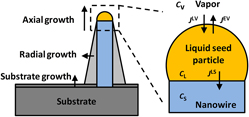
A cornerstone in the successful application of semiconductor nanowire devices is controlled impurity doping. In this review article, we discuss the key results in the field of semiconductor nanowire doping. Considerable development has recently taken place in this field, and half of the references in this review are less than 3 years old. We present a simple model for dopant incorporation during in situ doping of particle-assisted growth of nanowires. The effects of doping on nanowire growth are thoroughly discussed since many investigators have seen much stronger and more complex effects than those observed in thin-film growth. We also give an overview of methods of characterizing doping in nanowires since these in many ways define the boundaries of our current understanding.

Type
Reviews
Copyright
Copyright © Materials Research Society 2011

Access options

Get access to the full version of this content by using one of the access options below. (Log in options will check for institutional or personal access. Content may require purchase if you do not have access.)

Footnotes

This section of Journal of Materials Research is reserved for papers that are reviews of literature in a given area.

References

REFERENCES

1.Mårtensson, T., Svensson, C.P.T., Wacaser, B.A., Larsson, M.W., Seifert, W., Deppert, K., Gustafsson, A., Wallenberg, L.R., and Samuelson, L.: Epitaxial III-V nanowires on silicon. Nano Lett. 4, 1987 (2004).CrossRefGoogle Scholar
2.Bakkers, E.P.A.M., Borgström, M.T., and Verheijen, M.A.: Epitaxial growth of III-V nanowires on group IV substrates. MRS Bull. 32, 117 (2007).CrossRefGoogle Scholar
3.Cui, Y. and Lieber, C.M.: Functional nanoscale electronic devices assembled using silicon nanowire building blocks. Science 291, 851 (2001).CrossRefGoogle ScholarPubMed
4.Thelander, C., Mårtensson, T., Björk, M.T., Ohlsson, B.J., Larsson, M.W., Wallenberg, L.R., and Samuelson, L.: Single-electron transistors in heterostructure nanowires. Appl. Phys. Lett. 83, 2052 (2003).CrossRefGoogle Scholar
5.Nadj-Perge, S., Frolov, S.M., Bakkers, E.P., and Kouwenhoven, L.P.: Spin-orbit qubit in a semiconductor nanowire. Nature 468, 1084 (2010).CrossRefGoogle Scholar
6.Haraguchi, K., Katsuyama, T., Hiruma, K., and Ogawa, K.: GaAs p-n junction formed in quantum wire crystals. Appl. Phys. Lett. 60, 745 (1992).CrossRefGoogle Scholar
7.Cui, Y., Duan, X.F., Hu, J.T., and Lieber, C.M.: Doping and electrical transport in silicon nanowires. J. Phys. Chem. B 104, 5213 (2000).CrossRefGoogle Scholar
8.Kempa, T.J., Tian, B.Z., Kim, D.R., Hu, J.S., Zheng, X.L., and Lieber, C.M.: Single and tandem axial p-i-n nanowire photovoltaic devices. Nano Lett. 8, 3456 (2008).CrossRefGoogle ScholarPubMed
9.Minot, E.D., Kelkensberg, F., van Kouwen, M., van Dam, J.A., Kouwenhoven, L.P., Zwiller, V., Borgström, M.T., Wunnicke, O., Verheijen, M.A., and Bakkers, E.P.A.M.: Single quantum dot nanowire LEDs. Nano Lett. 7, 367 (2007).CrossRefGoogle ScholarPubMed
10.Björk, M.T., Knoch, J., Schmid, H., Riel, H., and Riess, W.: Silicon nanowire tunneling field-effect transistors. Appl. Phys. Lett. 92, 193504 (2008).CrossRefGoogle Scholar
11.Stringfellow, G.B.: The role of impurities in III/V semiconductors grown by organometallic vapor-phase epitaxy. J. Cryst. Growth 75, 91 (1986).CrossRefGoogle Scholar
12.Caroff, P., Bolinsson, J., and Johansson, J.: Crystal phases in III–V nanowires: From random toward engineered polytypism. IEEE J. Sel. Top. Quant. Electron. PP, 18 (2010).Google Scholar
13.Xu, L.A., Su, Y., Chen, Y.Q., Xiao, H.H., Zhu, L.A., Zhou, Q.T., and Li, S.: Synthesis and characterization of indium-doped ZnO nanowires with periodical single-twin structures. J. Phys. Chem. B 110, 6637 (2006).CrossRefGoogle ScholarPubMed
14.Algra, R.E., Verheijen, M.A., Borgström, M.T., Feiner, L-F., Immink, G., van Enckevort, W.J.P., Vlieg, E., and Bakkers, E.P.A.M.: Twinning superlattices in indium phosphide nanowires. Nature 456, 369 (2008).CrossRefGoogle ScholarPubMed
15.Seoane, N., Martinez, A., Brown, A.R., Barker, J.R., and Asenov, A.: Current variability in Si nanowire MOSFETs due to random dopants in the source/drain regions: A fully 3-D NEGF simulation study. IEEE Trans. Electron. Dev. 56, 1388 (2009).CrossRefGoogle Scholar
16.Zheng, G.F., Lu, W., Jin, S., and Lieber, C.M.: Synthesis and fabrication of high-performance n-type silicon nanowire transistors. Adv. Mater. 16, 1890 (2004).CrossRefGoogle Scholar
17.Kim, B.S., Koo, T.W., Lee, J.H., Kim, D.S., Jung, Y.C., Hwang, S.W., Choi, B.L., Lee, E.K., Kim, J.M., and Whang, D.: Catalyst-free growth of single-crystal silicon and germanium nanowires. Nano Lett. 9, 864 (2009).CrossRefGoogle ScholarPubMed
18.Schmid, H., Björk, M.T., Knoch, J., Riel, H., Riess, W., Rice, P., and Topuria, T.: Patterned epitaxial vapor-liquid-solid growth of silicon nanowires on Si(111) using silane. J. Appl. Phys. 103, 024304 (2008).CrossRefGoogle Scholar
19.Li, F., Nellist, P.D., and Cockayne, D.J.H.: Doping-dependent nanofaceting on silicon nanowire surfaces. Appl. Phys. Lett. 94, 263111 (2009).CrossRefGoogle Scholar
20.Schmid, H., Björk, M.T., Knoch, J., Karg, S., Riel, H., and Riess, W.: Doping limits of grown in situ doped silicon nanowires using phosphine. Nano Lett. 9, 173 (2009).CrossRefGoogle ScholarPubMed
21.Perea, D.E., Hemesath, E.R., Schwalbach, E.J., Lensch-Falk, J.L., Voorhees, P.W., and Lauhon, L.J.: Direct measurement of dopant distribution in an individual vapour-liquid-solid nanowire. Nat. Nanotechnol. 4, 315 (2009).CrossRefGoogle Scholar
22.Wang, Y.F., Lew, K.K., Ho, T.T., Pan, L., Novak, S.W., Dickey, E.C., Redwing, J.M., and Mayer, T.S.: Use of phosphine as an n-type dopant source for vapor-liquid-solid growth of silicon nanowires. Nano Lett. 5, 2139 (2005).CrossRefGoogle ScholarPubMed
23.Koren, E., Rosenwaks, Y., Allen, J.E., Hemesath, E.R., and Lauhon, L.J.: Nonuniform doping distribution along silicon nanowires measured by Kelvin probe force microscopy and scanning photocurrent microscopy. Appl. Phys. Lett. 95, 092105 (2009).CrossRefGoogle Scholar
24.Celle, C., Mouchet, C., Rouviere, E., Simonato, J.P., Mariolle, D., Chevalier, N., and Brioude, A.: Controlled in situ n-doping of silicon nanowires during VLS growth and their characterization by scanning spreading resistance microscopy. J. Phys. Chem. C 114, 760 (2010).CrossRefGoogle Scholar
25.Nimmatoori, P., Zhang, Q., Dickey, E.C., and Redwing, J.M.: Suppression of the vapor-liquid-solid growth of silicon nanowires by antimony addition. Nanotechnology 20, 025607 (2009).CrossRefGoogle ScholarPubMed
26.Imamura, G., Kawashima, T., Fujii, M., Nishimura, C., Saitoh, T., and Hayashi, S.: Distribution of active impurities in single silicon nanowires. Nano Lett. 8, 2620 (2008).CrossRefGoogle ScholarPubMed
27.Lauhon, L.J., Gudiksen, M.S., Wang, C.L., and Lieber, C.M.: Epitaxial core-shell and core-multishell nanowire heterostructures. Nature 420, 57 (2002).CrossRefGoogle ScholarPubMed
28.Lew, K.K., Pan, L., Bogart, T.E., Dilts, S.M., Dickey, E.C., Redwing, J.M., Wang, Y.F., Cabassi, M., Mayer, T.S., and Novak, S.W.: Structural and electrical properties of trimethylboron-doped silicon nanowires. Appl. Phys. Lett. 85, 3101 (2004).CrossRefGoogle Scholar
29.Givargizov, E.I.: Periodic instability in whisker growth. J. Cryst. Growth 20, 217 (1973).CrossRefGoogle Scholar
30.Wacaser, B.A., Reuter, M.C., Khayyat, M.M., Wen, C.Y., Haight, R., Guha, S., and Ross, F.M.: Growth system, structure, and doping of aluminum-seeded epitaxial silicon nanowires. Nano Lett. 9, 3296 (2009).CrossRefGoogle ScholarPubMed
31.Lee, W.F., Lee, C.Y., Ho, M.L., Huang, C.T., Lai, C.H., Hsieh, H.Y., Chou, P.T., and Chen, L.J.: Nd-doped silicon nanowires with room temperature ferromagnetism and infrared photoemission. Appl. Phys. Lett. 94, 263117 (2009).CrossRefGoogle Scholar
32.Kodambaka, S., Hannon, J.B., Tromp, R.M., and Ross, F.M.: Control of Si nanowire growth by oxygen. Nano Lett. 6, 1292 (2006).CrossRefGoogle ScholarPubMed
33.Greytak, A.B., Lauhon, L.J., Gudiksen, M.S., and Lieber, C.M.: Growth and transport properties of complementary germanium nanowire field-effect transistors. Appl. Phys. Lett. 84, 4176 (2004).CrossRefGoogle Scholar
34.Tutuc, E., Appenzeller, J., Reuter, M.C., and Guha, S.: Realization of a linear germanium nanowire p-n junction. Nano Lett. 6, 2070 (2006).CrossRefGoogle ScholarPubMed
35.Le, S.T., Jannaty, P., Zaslavsky, A., Dayeh, S.A., and Picraux, S.T.: Growth, electrical rectification, and gate control in axial in situ doped p-n junction germanium nanowires. Appl. Phys. Lett. 96, 262102 (2010).CrossRefGoogle Scholar
36.Wang, D. and Dai, H.: Germanium nanowires: From synthesis, surface chemistry, and assembly to devices. Appl. Phys. A 85, 217 (2006).CrossRefGoogle Scholar
37.Tutuc, E., Chu, J.O., Ott, J.A., and Guha, S.: Doping of germanium nanowires grown in presence of PH3. Appl. Phys. Lett. 89, 263101 (2006).CrossRefGoogle Scholar
38.Sutter, E. and Sutter, P.: Vapor-liquid-solid growth and Sb doping of Ge nanowires from a liquid Au-Sb-Ge ternary alloy. Appl. Phys. A 99, 217 (2010).CrossRefGoogle Scholar
39.Wang, D.W., Wang, Q., Javey, A., Tu, R., Dai, H.J., Kim, H., McIntyre, P.C., Krishnamohan, T., and Saraswat, K.C.: Germanium nanowire field-effect transistors with SiO2 and high-kappa HfO2 gate dielectrics. Appl. Phys. Lett. 83, 2432 (2003).CrossRefGoogle Scholar
40.Tutuc, E., Guha, S., and Chu, J.O.: Morphology of germanium nanowires grown in presence of B2H6. Appl. Phys. Lett. 88, 043113 (2006).CrossRefGoogle Scholar
41.Grossi, V., Bussolotti, F., Passacantando, M., Santucci, S., and Ottaviano, L.: Mn doping of germanium nanowires by vapour-liquid-solid deposition. Superlattices Microstruct. 44, 489 (2008).CrossRefGoogle Scholar
42.Choi, H.J., Seong, H.K., Lee, J.C., and Sung, Y.M.: Growth and modulation of silicon carbide nanowires. J. Cryst. Growth 269, 472 (2004).CrossRefGoogle Scholar
43.Yang, Y., Zhao, Q., Zhang, X.Z., Liu, Z.G., Zou, C.X., Shen, B., and Yu, D.P.: Mn-doped AIN nanowires with room temperature ferromagnetic ordering. Appl. Phys. Lett. 90, 092118 (2007).CrossRefGoogle Scholar
44.Liu, J., Meng, X.M., Jiang, Y., Lee, C.S., Bello, I., and Lee, S.T.: Gallium nitride nanowires doped with silicon. Appl. Phys. Lett. 83, 4241 (2003).CrossRefGoogle Scholar
45.Son, M.S., Im, S.I., Park, Y.S., Park, C.M., Kang, T.W., and Yoo, K.H.: Ultraviolet photodetector based on single GaN nanorod p-n junctions. Mater. Sci. Eng., C 26, 886 (2006).CrossRefGoogle Scholar
46.Guo, W., Zhang, M., Banerjee, A., and Bhattacharya, P.: Catalyst-free InGaN/GaN nanowire light emitting diodes grown on (001) silicon by molecular beam epitaxy. Nano Lett. 10, 3355 (2010).CrossRefGoogle ScholarPubMed
47.Furtmayr, F., Vielemeyer, M., Stutzmann, M., Laufer, A., Meyer, B.K., and Eickhoff, M.: Optical properties of Si- and Mg-doped gallium nitride nanowires grown by plasma-assisted molecular-beam epitaxy. J. Appl. Phys. 104, 074309 (2008).CrossRefGoogle Scholar
48.Qian, F., Li, Y., Gradecak, S., Wang, D.L., Barrelet, C.J., and Lieber, C.M.: Gallium nitride-based nanowire radial heterostructures for nanophotonics. Nano Lett. 4, 1975 (2004).CrossRefGoogle Scholar
49.Zhong, Z.H., Qian, F., Wang, D.L., and Lieber, C.M.: Synthesis of p-type gallium nitride nanowires for electronic and photonic nanodevices. Nano Lett. 3, 343 (2003).CrossRefGoogle Scholar
50.Cheng, G.S., Kolmakov, A., Zhang, Y.X., Moskovits, M., Munden, R., Reed, M.A., Wang, G.M., Moses, D., and Zhang, J.P.: Current rectification in a single GaN nanowire with a well-defined p-n junction. Appl. Phys. Lett. 83, 1578 (2003).CrossRefGoogle Scholar
51.Limbach, F., Schafer-Nolte, E.O., Caterino, R., Gotschke, T., Stoica, T., Sutter, E., and Calarco, R.: Morphology and optical properties of Mg doped GaN nanowires in dependence of growth temperature. J. Optoelectron. Adv. Mater. 12, 1433 (2010).Google Scholar
52.Tang, Y.B., Chen, Z.H., Song, H.S., Lee, C.S., Cong, H.T., Cheng, H.M., Zhang, W.J., Bello, I., and Lee, S.T.: Vertically aligned p-type single-crystalline GaN nanorod arrays on n-type Si for heterojunction photovoltaic cells. Nano Lett. 8, 4191 (2008).CrossRefGoogle ScholarPubMed
53.Zhou, S.M.: Near UV photoluminescence of Hg-doped GaN nanowires. Physica E 33, 394 (2006).CrossRefGoogle Scholar
54.Han, D.S., Park, J., Rhie, K.W., Kim, S., and Chang, J.: Ferromagnetic Mn-doped GaN nanowires. Appl. Phys. Lett. 86, 032506 (2005).CrossRefGoogle Scholar
55.Radovanovic, P.V., Stamplecoskie, K.G., and Pautler, B.G.: Dopant ion concentration dependence of growth and faceting of manganese-doped GaN nanowires. J. Am. Chem. Soc. 129, 10980 (2007).CrossRefGoogle ScholarPubMed
56.Chen, Z.G., Cheng, L.N., Lu, G.Q., and Zou, J.: Sulfur-doped gallium phosphide nanowires and their optoelectronic properties. Nanotechnology 21, 375701 (2010).CrossRefGoogle ScholarPubMed
57.Seo, H.W., Bae, S.Y., Park, J., Kang, M.I., and Kim, S.: Nitrogen-doped gallium phosphide nanowires. Chem. Phys. Lett. 378, 420 (2003).CrossRefGoogle Scholar
58.Han, D.S., Bae, S.Y., Seo, H.W., Kang, Y.J., Park, J., Lee, G., Ahn, J.P., Kim, S., and Chang, J.: Synthesis and magnetic properties of manganese-doped GaP nanowires. J. Phys. Chem. B. 109, 9311 (2005).CrossRefGoogle ScholarPubMed
59.Lee, H.G., Jeon, H.C., Kang, T.W., and Kim, T.W.: Gallium arsenide crystalline nanorods grown by molecular-beam epitaxy. Appl. Phys. Lett. 78, 3319 (2001).CrossRefGoogle Scholar
60.Hilse, M., Ramsteiner, M., Breuer, S., Geelhaar, L., and Riechert, H.: Incorporation of the dopants Si and Be into GaAs nanowires. Appl. Phys. Lett. 96, 193104 (2010).CrossRefGoogle Scholar
61.Colombo, C., Heibeta, M., Gratzel, M., and Fontcuberta i Morral, A.: Gallium arsenide p-i-n radial structures for photovoltaic applications. Appl. Phys. Lett. 94, 173108 (2009).CrossRefGoogle Scholar
62.Tomioka, K., Motohisa, J., Hara, S., Hiruma, K., and Fukui, T.: GaAs/AlGaAs core multishell nanowire-based light-emitting diodes on Si. Nano Lett. 10, 1639 (2010).CrossRefGoogle ScholarPubMed
63.Sladek, K., Klinger, V., Wensorra, J., Akabori, M., Hardtdegen, H., and Grutzmacher, D.: MOVPE of n-doped GaAs and modulation doped GaAs/AlGaAs nanowires. J. Cryst. Growth 312, 635 (2010).CrossRefGoogle Scholar
64.Czaban, J.A., Thompson, D.A., and LaPierre, R.R.: GaAs core-shell nanowires for photovoltaic applications. Nano Lett. 9, 148 (2009).CrossRefGoogle ScholarPubMed
65.Caram, J., Sandoval, C., Tirado, M., Comedi, D., Czaban, J., Thompson, D.A., and LaPierre, R.R.: Electrical characteristics of core-shell p-n GaAs nanowire structures with Te as the n-dopant. Nanotechnology 21, 134007 (2010).CrossRefGoogle Scholar
66.Dufouleur, J., Colombo, C., Garma, T., Ketterer, B., Uccelli, E., Nicotra, M., and Morral, A.F.I.: P-doping mechanisms in catalyst-free gallium arsenide nanowires. Nano Lett. 10, 1734 (2010).CrossRefGoogle ScholarPubMed
67.Ketterer, B., Mikheev, E., Uccelli, E., and Fontcuberta i Morral, A.: Compensation mechanism in silicon-doped gallium arsenide nanowires. Appl. Phys. Lett. 97, 223103 (2010).CrossRefGoogle Scholar
68.Gutsche, C., Regolin, I., Blekker, K., Lysov, A., Prost, W., and Tegude, F.J.: Controllable p-type doping of GaAs nanowires during vapor-liquid-solid growth. J. Appl. Phys. 105, 024305 (2009).CrossRefGoogle Scholar
69.Wallentin, J., Persson, J.M., Wagner, J.B., Samuelson, L., Deppert, K., and Borgström, M.T.: High-performance single nanowire tunnel diodes. Nano Lett. 10, 974 (2010).CrossRefGoogle ScholarPubMed
70.Martelli, F., Rubini, S., Piccin, M., Bais, G., Jabeen, F., De Franceschi, S., Grillo, V., Carlino, E., D’Acapito, F., Boscherini, F., Cabrini, S., Lazzarino, M., Businaro, L., Romanato, F., and Franciosi, A.: Manganese-induced growth of GaAs nanowires. Nano Lett. 6, 2130 (2006).CrossRefGoogle ScholarPubMed
71.Richter, T., Luth, H., Schapers, T., Meijers, R., Jeganathan, K., Hernandez, S.E., Calarco, R., and Marso, M.: Electrical transport properties of single undoped and n-type doped InN nanowires. Nanotechnology 20, 405206 (2009).CrossRefGoogle ScholarPubMed
72.Cusco, R., Domenech-Amador, N., Artus, L., Gotschke, T., Jeganathan, K., Stoica, T., and Calarco, R.: Probing the electron density in undoped, Si-doped, and Mg-doped InN nanowires by means of Raman scattering. Appl. Phys. Lett. 97, 221906 (2010).CrossRefGoogle Scholar
73.Song, H.P., Yang, A.L., Zhang, R.Q., Guo, Y., Wei, H.Y., Zheng, G.L., Yang, S.Y., Liu, X.L., Zhu, Q.S., and Wang, Z.G.: Well-aligned Zn-doped InN nanorods grown by metal-organic chemical vapor deposition and the dopant distribution. Cryst. Growth Des. 9, 3292 (2009).CrossRefGoogle Scholar
74.Rigutti, L., Bugallo, A.D., Tchernycheva, M., Jacopin, G., Julien, F.H., Cirlin, G., Patriarche, G., Lucot, D., Travers, L., and Harmand, J.C.: Si incorporation in InP nanowires grown by Au-assisted molecular beam epitaxy. J. Nanomater. 2009, 435451 (2009).CrossRefGoogle Scholar
75.Goto, H., Nosaki, K., Tomioka, K., Hara, S., Hiruma, K., Motohisa, J., and Fukui, T.: growth of core–shell InP nanowires for photovoltaic application by selective-area metal organic vapor phase epitaxy. Appl. Phys. Express 2, 035004 (2009).CrossRefGoogle Scholar
76.Duan, X.F., Huang, Y., Cui, Y., Wang, J.F., and Lieber, C.M.: Indium phosphide nanowires as building blocks for nanoscale electronic and optoelectronic devices. Nature 409, 66 (2001).CrossRefGoogle ScholarPubMed
77.Borgström, M.T., Norberg, E., Wickert, P., Nilsson, H.A., Trägårdh, J., Dick, K.A., Statkute, G., Ramvall, P., Deppert, K., and Samuelson, L.: Precursor evaluation for in situ InP nanowire doping. Nanotechnology 19, 445602 (2008).CrossRefGoogle ScholarPubMed
78.van Weert, M.H.M., Helman, A., van den Einden, W., Algra, R.E., Verheijen, M.A., Borgström, M.T., Immink, G., Kelly, J.J., Kouwenhoven, L.P., and Bakkers, E.P.A.M.: Zinc incorporation via the vapor-liquid-solid mechanism into InP nanowires. J. Am. Chem. Soc. 131, 4578 (2009).CrossRefGoogle ScholarPubMed
79.Wallentin, J., Mergenthaler, K., Ek, M., Wallenberg, L.R., Samuelson, L., Deppert, K., Pistol, M.-E., and Borgström, M.T.: Probing the wurtzite conduction band structure using state-filling in highly doped InP nanowires. Nano Lett. 11, 2286 (2011).CrossRefGoogle ScholarPubMed
80.De Franceschi, S., van Dam, J.A., Bakkers, E., Feiner, L.F., Gurevich, L., and Kouwenhoven, L.P.: Single-electron tunneling in InP nanowires. Appl. Phys. Lett. 83, 344 (2003).CrossRefGoogle Scholar
81.Liu, C., Dai, L., You, L.P., Xu, W.J., and Qin, G.G.: Blueshift of electroluminescence from single n-InP nanowire/p-Si heterojunctions due to the Burstein–Moss effect. Nanotechnology 19, 465203 (2008).CrossRefGoogle Scholar
82.van Weert, M.H.M., Wunnicke, O., Roest, A.L., Eijkemans, T.J., Yu Silov, A., and Haverkort, J.E.M., ’t Hooft, G.W., Bakkers, E.P.A.M.: Large redshift in photoluminescence of p-doped InP nanowires induced by Fermi-level pinning. Appl. Phys. Lett. 88, 043109 (2006).CrossRefGoogle Scholar
83.Wallentin, J., Ek, M., Wallenberg, L.R., Samuelson, L., Deppert, K., and Borgström, M.T.: Changes in contact angle of seed particle correlated with increased zincblende formation in doped InP nanowires. Nano Lett. 10, 4807 (2010).CrossRefGoogle ScholarPubMed
84.Borgström, M.T., Wallentin, J., Heurlin, M., Fält, S., Wickert, P., Leene, J., Magnusson, M.H., Deppert, K., and Samuelson, L.: Nanowires With Promise for Photovoltaics. IEEE Journal of Selected Topics in Quantum Electronics 17, 1050 (2011).CrossRefGoogle Scholar
85.Thelander, C., Dick, K.A., Borgström, M.T., Fröberg, L.E., Caroff, P., Nilsson, H.A., and Samuelson, L.: The electrical and structural properties of n-type InAs nanowires grown from metal-organic precursors. Nanotechnology 21, 205703 (2010).CrossRefGoogle ScholarPubMed
86.Sorensen, B.S., Aagesen, M., Sorensen, C.B., Lindelof, P.E., Martinez, K.L., and Nygard, J.: Ambipolar transistor behavior in p-doped InAs nanowires grown by molecular beam epitaxy. Appl. Phys. Lett. 92, 012119 (2008).CrossRefGoogle Scholar
87.Geng, B.Y., Wang, G.Z., Jiang, Z., Xie, T., Sun, S.H., Meng, G.W., and Zhang, L.D.: Synthesis and optical properties of S-doped ZnO nanowires. Appl. Phys. Lett. 82, 4791 (2003).CrossRefGoogle Scholar
88.Bae, S.Y., Seo, H.W., and Park, J.H.: Vertically aligned sulfur-doped ZnO nanowires synthesized via chemical vapor deposition. J. Phys. Chem. B 108, 5206 (2004).CrossRefGoogle Scholar
89.Li, S.Y., Lin, P., Lee, C.Y., Tseng, T.Y., and Huang, C.J.: Effect of Sn dopant on the properties of ZnO nanowires. J. Phys. D 37, 2274 (2004).CrossRefGoogle Scholar
90.Gao, J.Y., Zhang, X.Z., Sun, Y.H., Zhao, Q., and Yu, D.P.: Compensation mechanism in N-doped ZnO nanowires. Nanotechnology 21, 245703 (2010).CrossRefGoogle ScholarPubMed
91.Yuan, G.D., Zhang, W.J., Jie, J.S., Fan, X., Tang, J.X., Shafiq, I., Ye, Z.Z., Lee, C.S., and Lee, S.T.: Tunable n-type conductivity and transport properties of Ga-doped ZnO nanowire arrays. Adv. Mater. 20, 168 (2008).CrossRefGoogle Scholar
92.Liu, C.H., Yiu, W.C., Au, F.C.K., Ding, J.X., Lee, C.S., and Lee, S.T.: Electrical properties of zinc oxide nanowires and intramolecular p-n junctions. Appl. Phys. Lett. 83, 3168 (2003).CrossRefGoogle Scholar
93.Xiang, B., Wang, P.W., Zhang, X.Z., Dayeh, S.A., Aplin, D.P.R., Soci, C., Yu, D.P., and Wang, D.L.: Rational synthesis of p-type zinc oxide nanowire arrays using simple chemical vapor deposition. Nano Lett. 7, 323 (2007).CrossRefGoogle ScholarPubMed
94.Li, P.J., Liao, Z.M., Zhang, X.Z., Zhang, X.J., Zhu, H.C., Gao, J.Y., Laurent, K., Leprince-Wang, Y., Wang, N., and Yu, D.P.: Electrical and photoresponse properties of an intramolecular p-n homojunction in single phosphorus-doped ZnO nanowires. Nano Lett. 9, 2513 (2009).CrossRefGoogle ScholarPubMed
95.Yuan, G.D., Zhang, W.J., Jie, J.S., Fan, X., Zapien, J.A., Leung, Y.H., Luo, L.B., Wang, P.F., Lee, C.S., and Lee, S.T.: P-type ZnO nanowire arrays. Nano Lett. 8, 2591 (2008).CrossRefGoogle ScholarPubMed
96.Liu, W., Xiu, F.X., Sun, K., Xie, Y.H., Wang, K.L., Wang, Y., Zou, J., Yang, Z., and Liu, J.L.: Na-doped p-type ZnO microwires. J. Am. Chem. Soc. 132, 2498 (2010).CrossRefGoogle ScholarPubMed
97.Chang, Y.Q., Wang, D.B., Luo, X.H., Xu, X.Y., Chen, X.H., Li, L., Chen, C.P., Wang, R.M., Xu, J., and Yu, D.P.: Synthesis, optical, and magnetic properties of diluted magnetic semiconductor Zn1-x MnxO nanowires via vapor phase growth. Appl. Phys. Lett. 83, 4020 (2003).CrossRefGoogle Scholar
98.Liu, J.J., Yu, M.H., and Zhou, W.L.: Well-aligned Mn-doped ZnO nanowires synthesized by a chemical-vapor-deposition method. Appl. Phys. Lett. 87, 172505 (2005).CrossRefGoogle Scholar
99.Radovanovic, P.V., Barrelet, C.J., Gradecak, S., Qian, F., and Lieber, C.M.: General synthesis of manganese-doped II-VI and III-V semiconductor nanowires. Nano Lett. 5, 1407 (2005).CrossRefGoogle ScholarPubMed
100.Willander, M., Nur, O., Zhao, Q.X., Yang, L.L., Lorenz, M., Cao, B.Q., Perez, J.Z., Czekalla, C., Zimmermann, G., Grundmann, M., Bakin, A., Behrends, A., Al-Suleiman, M., El-Shaer, A., Mofor, A.C., Postels, B., Waag, A., Boukos, N., Travlos, A., Kwack, H.S., Guinard, J., and Dang, D.L.: Zinc oxide nanorod based photonic devices: Recent progress in growth, light emitting diodes and lasers. Nanotechnology 20, 332001 (2009).CrossRefGoogle ScholarPubMed
101.Fan, Z.Y. and Lu, J.G.: Zinc oxide nanostructures: Synthesis and properties. J. Nanosci. Nanotechnol 5, 1561 (2005).CrossRefGoogle ScholarPubMed
102.Chen, Y.Q., Jiang, J., Wang, B., and Hou, J.G.: Synthesis of tin-doped indium oxide nanowires by self-catalytic VLS growth. J. Phys. D: Appl. Phys. 37, 3319 (2004).CrossRefGoogle Scholar
103.Wan, Q., Song, Z.T., Feng, S.L., and Wang, T.H.: Single-crystalline tin-doped indium oxide whiskers: Synthesis and characterization. Appl. Phys. Lett. 85, 4759 (2004).CrossRefGoogle Scholar
104.Wan, Q., Dattoli, E.N., Fung, W.Y., Guo, W., Chen, Y.B., Pan, X.Q., and Lu, W.: High-performance transparent conducting oxide nanowires. Nano Lett. 6, 2909 (2006).CrossRefGoogle ScholarPubMed
105.Nguyen, P., Ng, H.T., Kong, J., Cassell, A.M., Quinn, R., Li, J., Han, J., McNeil, M., and Meyyappan, M.: Epitaxial directional growth of indium-doped tin oxide nanowire arrays. Nano Lett. 3, 925 (2003).CrossRefGoogle Scholar
106.Wan, Q., Dattoli, E.N., and Lu, W.: Transparent metallic Sb-doped SnO2 nanowires. Appl. Phys. Lett. 90, 222107 (2007).CrossRefGoogle Scholar
107.Klamchuen, A., Yanagida, T., Nagashima, K., Seki, S., Oka, K., Taniguchi, M., and Kawai, T.: Crucial role of doping dynamics on transport properties of Sb-doped SnO2 nanowires. Appl. Phys. Lett. 95, 053105 (2009).CrossRefGoogle Scholar
108.Jie, J.S., Zhang, W.J., Bello, I., Lee, C.S., and Lee, S.T.: One-dimensional II-VI nanostructures: Synthesis, properties and optoelectronic applications. Nano Today 5, 313 (2010).CrossRefGoogle Scholar
109.Wacaser, B.A., Dick, K.A., Johansson, J., Borgström, M.T., Deppert, K., and Samuelson, L.: Preferential interface nucleation: An expansion of the VLS growth mechanism for nanowires. Adv. Mater. 21, 153 (2009).CrossRefGoogle Scholar
110.Dick, K.A.: A review of nanowire growth promoted by alloys and non-alloying elements with emphasis on Au-assisted III-V nanowires. Prog. Cryst. Growth Charact. Mater. 54, 138 (2008).CrossRefGoogle Scholar
111.Allen, J.E., Perea, D.E., Hemesath, E.R., and Lauhon, L.J.: Nonuniform nanowire doping profiles revealed by quantitative scanning photocurrent microscopy. Adv. Mater. 21, 3067 (2009).CrossRefGoogle Scholar
112.Verheijen, M.A., Immink, G., de Smet, T., Borgström, M.T., and Bakkers, E.P.A.M.: Growth kinetics of heterostructured GaP–GaAs nanowires. J. Am. Chem. Soc. 128, 1353 (2006).CrossRefGoogle ScholarPubMed
113.Borgström, M.T., Wallentin, J., Trägårdh, J., Ramvall, P., Ek, M., Wallenberg, L.R., Samuelson, L., and Deppert, K.: In situ etching for total control over axial and radial nanowire growth. Nano Research 3, 264 (2010).CrossRefGoogle Scholar
114.Kuphal, E.: Preparation and characterization of LPE InP. J. Cryst. Growth 54, 117 (1981).CrossRefGoogle Scholar
115.Logan, R.A., Tanbunek, T., and Sergent, A.M.: Doping of InP and GaInAs with S during metalorganic vapor phase epitaxy. J. Appl. Phys. 65, 3723 (1989).CrossRefGoogle Scholar
116.Li, N., Tan, T.Y., and Gösele, U.: Transition region width of nanowire hetero- and pn-junctions grown using vapor–liquid–solid processes. Appl. Phys. A 90, 591 (2008).CrossRefGoogle Scholar
117.Björk, M.T., Ohlsson, B.J., Sass, T., Persson, A.I., Thelander, C., Magnusson, M.H., Deppert, K., Wallenberg, L.R., and Samuelson, L.: One-dimensional heterostructures in semiconductor nanowhiskers. Appl. Phys. Lett. 80, 1058 (2002).CrossRefGoogle Scholar
118.Borgström, M.T., Verheijen, M.A., Immink, G., de Smet, T., and Bakkers, E.P.A.M.: Interface study on heterostructured GaP–GaAs nanowires. Nanotechnology 17, 4010 (2006).CrossRefGoogle Scholar
119.Fröberg, L.E., Wacaser, B.A., Wagner, J.B., Jeppesen, S., Ohlsson, B.J., Deppert, K., and Samuelson, L.: Transients in the formation of nanowire heterostructures. Nano Lett. 8, 3815 (2008).CrossRefGoogle ScholarPubMed
120.Wen, C.Y., Reuter, M.C., Bruley, J., Tersoff, J., Kodambaka, S., Stach, E.A., and Ross, F.M.: Formation of compositionally abrupt axial heterojunctions in silicon-germanium nanowires. Science 326, 1247 (2009).CrossRefGoogle ScholarPubMed
121.Glas, F., Harmand, J-C., and Patriarche, G.: Nucleation antibunching in catalyst-assisted nanowire growth. Phys. Rev. Lett. 104, 135501 (2010).CrossRefGoogle ScholarPubMed
122.Peelaers, H., Partoens, B., and Peeters, F.M.: Formation and segregation energies of B and P doped and BP codoped silicon nanowires. Nano Lett. 6, 2781 (2006).CrossRefGoogle ScholarPubMed
123.Fernandez-Serra, M.V., Adessi, C., and Blase, X.: Surface segregation and backscattering in doped silicon nanowires. Phys. Rev. Lett. 96, 166805 (2006).CrossRefGoogle ScholarPubMed
124.Xie, P., Hu, Y.J., Fang, Y., Huang, J.L., and Lieber, C.M.: Diameter-dependent dopant location in silicon and germanium nanowires. Proc. Natl. Acad. Sci. USA 106, 15254 (2009).CrossRefGoogle ScholarPubMed
125.Johansson, J., Karlsson, L.S., Svensson, C.P.T., Mårtensson, T., Wacaser, B.A., Deppert, K., Samuelson, L., and Seifert, W.: Structural properties of (111)B-oriented III-V nanowires. Nat. Mater. 5, 574 (2006).CrossRefGoogle Scholar
126.Chichibu, S., Kushibe, M., Eguchi, K., Funemizu, M., and Ohba, Y.: High-concentration Zn doping in Inp grown by low-pressure metalorganic chemical vapor-deposition. J. Appl. Phys. 68, 859 (1990).CrossRefGoogle Scholar
127.Diarra, M., Niquet, Y.M., Delerue, C., and Allan, G.: Ionization energy of donor and acceptor impurities in semiconductor nanowires: Importance of dielectric confinement. Phys. Rev. B 75, 045301 (2007).CrossRefGoogle Scholar
128.Björk, M.T., Schmid, H., Knoch, J., Riel, H., and Riess, W.: Donor deactivation in silicon nanostructures. Nat. Nanotechnol. 4, 103 (2009).CrossRefGoogle ScholarPubMed
129.Hong, K-H., Kim, J., Lee, J.H., Shin, J., and Chung, U.I.: Asymmetric doping in silicon nanostructures: the impact of surface dangling bonds. Nano Lett. 10, 1671 (2010).CrossRefGoogle ScholarPubMed
130.Arbiol, J., Estrade, S., Prades, J.D., Cirera, A., Furtmayr, F., Stark, C., Laufer, A., Stutzmann, M., Eickhoff, M., Gass, M.H., Bleloch, A.L., Peiro, F., and Morante, J.R.: Triple-twin domains in Mg doped GaN wurtzite nanowires: Structural and electronic properties of this zinc-blende-like stacking. Nanotechnology 20, 145704 (2009).CrossRefGoogle ScholarPubMed
131.Liu, B.D., Bando, Y., Tang, C.C., Xu, F.F., and Golberg, D.: Excellent field-emission properties of P-doped GaN nanowires. J. Phys. Chem. B 109, 21521 (2005).CrossRefGoogle ScholarPubMed
132.Ford, A.C., Chuang, S., Ho, J.C., Chueh, Y.L., Fan, Z.Y., and Javey, A.: Patterned p-doping of InAs nanowires by gas-phase surface diffusion of Zn. Nano Lett. 10, 509 (2010).CrossRefGoogle ScholarPubMed
133.Moselund, K.E., Ghoneim, H., Schmid, H., Björk, M.T., Lortscher, E., Karg, S., Signorello, G., Webb, D., Tschudy, M., Beyeler, R., and Riel, H.: Solid-state diffusion as an efficient doping method for silicon nanowires and nanowire field effect transistors. Nanotechnology 21, 435202 (2010).CrossRefGoogle ScholarPubMed
134.Ho, J.C., Yerushalmi, R., Jacobson, Z.A., Fan, Z., Alley, R.L., and Javey, A.: Controlled nanoscale doping of semiconductors via molecular monolayers. Nat. Mater. 7, 62 (2008).CrossRefGoogle ScholarPubMed
135.Dhara, S., Datta, A., Wu, C.T., Lan, Z.H., Chen, K.H., Wang, Y.L., Chen, Y.F., Hsu, C.W., Chen, L.C., Lin, H.M., and Chen, C.C.: Blueshift of yellow luminescence band in self-ion-implanted n-GaN nanowire. Appl. Phys. Lett. 84, 3486 (2004).CrossRefGoogle Scholar
136.Hayden, O., Björk, M.T., Schmid, H., Riel, H., Drechsler, U., Karg, S.F., Lortscher, E., and Riess, W.: Fully depleted nanowire field-effect transistor in inversion mode. Small 3, 230 (2007).CrossRefGoogle ScholarPubMed
137.Cohen, G.M., Rooks, M.J., Chu, J.O., Laux, S.E., Solomon, P.M., Ott, J.A., Miller, R.J., and Haensch, W.: Nanowire metal-oxide-semiconductor field effect transistor with doped epitaxial contacts for source and drain. Appl. Phys. Lett. 90, 233110 (2007).CrossRefGoogle Scholar
138.Stichtenoth, D., Wegener, K., Gutsche, C., Regolin, I., Tegude, F.J., Prost, W., Seibt, M., and Ronning, C.: P-type doping of GaAs nanowires. Appl. Phys. Lett. 92, 163107 (2008).CrossRefGoogle Scholar
139.Colli, A., Fasoli, A., Ronning, C., Pisana, S., Piscanec, S., and Ferrari, A.C.: Ion beam doping of silicon nanowires. Nano Lett. 8, 2188 (2008).CrossRefGoogle ScholarPubMed
140.Das Kanungo, P., Kögler, R., Nguyen-Duc, K., Zakharov, N., Werner, P., and Gösele, U.: Ex situ n and p doping of vertical epitaxial short silicon nanowires by ion implantation. Nanotechnology 20, 165706 (2009).CrossRefGoogle Scholar
141.Hoffmann, S., Bauer, J., Ronning, C., Stelzner, T., Michler, J., Ballif, C., Sivakov, V., and Christiansen, S.H.: Axial p-n junctions realized in silicon nanowires by ion implantation. Nano Lett. 9, 1341 (2009).CrossRefGoogle ScholarPubMed
142.Li, H.Y., Wunnicke, O., Borgström, M.T., Immink, W.G.G., van Weert, M.H.M., Verheijen, M.A., and Bakkers, E.: Remote p-doping of InAs nanowires. Nano Lett. 7, 1144 (2007).CrossRefGoogle ScholarPubMed
143.Simon, J., Protasenko, V., Lian, C., Xing, H., and Jena, D.: Polarization-induced hole doping in wide-band-gap uniaxial semiconductor heterostructures. Science 327, 60 (2010).CrossRefGoogle ScholarPubMed
144.Boxberg, F., Søndergaard, N., and Xu, H.Q.: Photovoltaics with piezoelectric core-shell nanowires. Nano Lett. 10, 1108 (2010).CrossRefGoogle ScholarPubMed
145.Kim, J.R., Kim, B.K., Lee, I.J., Kim, J.J., Kim, J., Lyu, S.C., and Lee, C.J.: Temperature-dependent single-electron tunneling effect in lightly and heavily doped GaN nanowires. Phys. Rev. B 69, 233303 (2004).CrossRefGoogle Scholar
146.Stern, E., Cheng, G., Cimpoiasu, E., Klie, R., Guthrie, S., Klemic, J., Kretzschmar, I., Steinlauf, E., Turner-Evans, D., Broomfield, E., Hyland, J., Koudelka, R., Boone, T., Young, M., Sanders, A., Munden, R., Lee, T., Routenberg, D., and Reed, M.A.: Electrical characterization of single GaN nanowires. Nanotechnology 16, 2941 (2005).CrossRefGoogle Scholar
147.Sze, S.: Physics of Semiconductor Devices (Wiley, New York, 1981).Google Scholar
148.Morse, P.M. and Feshbach, H.: Methods of Theoretical Physics (McGraw-Hill, New York, 1953).Google Scholar
149.Ng, H.T., Han, J., Yamada, T., Nguyen, P., Chen, Y.P., and Meyyappan, M.: Single crystal nanowire vertical surround-gate field-effect transistor. Nano Lett. 4, 1247 (2004).CrossRefGoogle Scholar
150.Wunnicke, O.: Gate capacitance of back-gated nanowire field-effect transistors. Appl. Phys. Lett. 89, 083102 (2006).CrossRefGoogle Scholar
151.Khanal, D.R. and Wu, J.: Gate coupling and charge distribution in nanowire field effect transistors. Nano Lett. 7, 2778 (2007).CrossRefGoogle ScholarPubMed
152.Kretinin, A.V., Popovitz-Biro, R., Mahalu, D., and Shtrikman, H.: Multimode Fabry-Perot conductance oscillations in suspended stacking-faults-free InAs nanowires. Nano Lett. 10, 3439 (2010).CrossRefGoogle ScholarPubMed
153.Park, H., Beresford, R., Hong, S., and Xu, J.: Geometry- and size-dependence of electrical properties of metal contacts on semiconducting nanowires. J. Appl. Phys. 108, 094308 (2010).CrossRefGoogle Scholar
154.Ivey, D.G., Jian, P., Wan, L., Bruce, R., Eicher, S., and Blaauw, C.: Pd/Zn/Pd/Au ohmic contacts to p-type Inp. J. Electron. Mater. 20, 237 (1991).CrossRefGoogle Scholar
155.Cui, Y., Zhong, Z.H., Wang, D.L., Wang, W.U., and Lieber, C.M.: High performance silicon nanowire field effect transistors. Nano Lett. 3, 149 (2003).CrossRefGoogle Scholar
156.Huang, Y., Duan, X., Cui, Y., and Lieber, C.M.: Gallium nitride nanowire nanodevices. Nano Lett. 2, 101 (2002).CrossRefGoogle Scholar
157.Leonard, F. and Talin, A.A.: Size-dependent effects on electrical contacts to nanotubes and nanowires. Phys. Rev. Lett. 97, 026804 (2006).CrossRefGoogle ScholarPubMed
158.Thelander, C., Björk, M.T., Larsson, M.W., Hansen, A.E., Wallenberg, L.R., and Samuelson, L.: Electron transport in InAs nanowires and heterostructure nanowire devices. Solid State Commun. 131, 573 (2004).CrossRefGoogle Scholar
159.Zhang, Z.Y., Yao, K., Liu, Y., Jin, C.H., Liang, X.L., Chen, Q., and Peng, L.M.: Quantitative analysis of current-voltage characteristics of semiconducting nanowires: Decoupling of contact effects. Adv. Funct. Mater. 17, 2478 (2007).CrossRefGoogle Scholar
160.Weber, W.M., Geelhaar, L., Unger, E., Cheze, C., Kreupl, F., Riechert, H., and Lugli, P.: Silicon to nickel-silicide axial nanowire heterostructures for high performance electronics. Phys. Status Solidi B Basic Res. 244, 4170 (2007).CrossRefGoogle Scholar
161.Tu, R., Zhang, L., Nishi, Y., and Dai, H.J.: Measuring the capacitance of individual semiconductor nanowires for carrier mobility assessment. Nano Lett. 7, 1561 (2007).CrossRefGoogle ScholarPubMed
162.Roddaro, S., Nilsson, K., Astromskas, G., Samuelson, L., Wernersson, L.E., Karlström, O., and Wacker, A.: InAs nanowire metal-oxide-semiconductor capacitors. Appl. Phys. Lett. 92, 253509 (2008).CrossRefGoogle Scholar
163.Karlström, O., Wacker, A., Nilsson, K., Astromskas, G., Roddaro, S., Samuelson, L., and Wernersson, L.E.: Analysing the capacitance-voltage measurements of vertical wrapped-gated nanowires. Nanotechnology 19, 435201 (2008).CrossRefGoogle ScholarPubMed
164.Astromskas, G., Storm, K., Karlström, O., Caroff, P., Borgström, M., and Wernersson, L-E.: Doping incorporation in InAs nanowires characterized by capacitance measurements. J. Appl. Phys. 108, 054306 (2010).CrossRefGoogle Scholar
165.Garnett, E.C., Tseng, Y.C., Khanal, D.R., Wu, J.Q., Bokor, J., and Yang, P.D.: Dopant profiling and surface analysis of silicon nanowires using capacitance-voltage measurements. Nat. Nanotechnol. 4, 311 (2009).CrossRefGoogle ScholarPubMed
166.Bakkers, E.P.A.M., Van Dam, J.A., De Franceschi, S., Kouwenhoven, L.P., Kaiser, M., Verheijen, M., Wondergem, H., and Van der Sluis, P.: Epitaxial growth of InP nanowires on germanium. Nat. Mater. 3, 769 (2004).CrossRefGoogle ScholarPubMed
167.Bugajski, M. and Lewandowski, W.: Concentration-dependent absorption and photoluminescence of n-type InP. J. Appl. Phys. 57, 521 (1985).CrossRefGoogle Scholar
168.Kawashima, T., Imamura, G., Saitoh, T., Komori, K., Fujii, M., and Hayashi, S.: Raman scattering studies of electrically active impurities in in situ B-Doped silicon nanowires: Effects of annealing and oxidation. J. Phys. Chem. C 111, 15160 (2007).CrossRefGoogle Scholar
169.Jeganathan, K., Debnath, R.K., Meijers, R., Stoica, T., Calarco, R., Grutzmacher, D., and Luth, H.: Raman scattering of phonon-plasmon coupled modes in self-assembled GaN nanowires. J. Appl. Phys. 105, 123707 (2009).CrossRefGoogle Scholar
170.Parkinson, P., Joyce, H.J., Gao, Q., Tan, H.H., Zhang, X., Zou, J., Jagadish, C., Herz, L.M., and Johnston, M.B.: Carrier lifetime and mobility enhancement in nearly defect-free core-shell nanowires measured using time-resolved terahertz spectroscopy. Nano Lett. 9, 3349 (2009).CrossRefGoogle ScholarPubMed
171.Richter, T., Luth, H., Meijers, R., Calarco, R., and Marso, M.: doping concentration of gan nanowires determined by opto-electrical measurements. Nano Lett. 8, 3056 (2008).CrossRefGoogle ScholarPubMed
172.Sanford, N.A., Blanchard, P.T., Bertness, K.A., Mansfield, L., Schlager, J.B., Sanders, A.W., Roshko, A., Burton, B.B., and George, S.M.: Steady-state and transient photoconductivity in c-axis GaN nanowires grown by nitrogen-plasma-assisted molecular-beam epitaxy. J. Appl. Phys. 107, 034318 (2010).CrossRefGoogle Scholar
173.Putnam, M.C., Filler, M.A., Kayes, B.M., Kelzenberg, M.D., Guan, Y.B., Lewis, N.S., Eiler, J.M., and Atwater, H.A.: Secondary ion mass spectrometry of vapor-liquid-solid grown, Au-catalyzed, Si wires. Nano Lett. 8, 3109 (2008).CrossRefGoogle ScholarPubMed
174.Perea, D.E., Allen, J.E., May, S.J., Wessels, B.W., Seidman, D.N., and Lauhon, L.J.: Three-dimensional nanoscale composition mapping of semiconductor nanowires. Nano Lett. 6, 181 (2006).CrossRefGoogle ScholarPubMed
175.Allen, J.E., Hemesath, E.R., Perea, D.E., Lensch-Falk, J.L., Li, Z.Y., Yin, F., Gass, M.H., Wang, P., Bleloch, A.L., Palmer, R.E., and Lauhon, L.J.: High-resolution detection of Au catalyst atoms in Si nanowires. Nat. Nanotechnol. 3, 168 (2008).CrossRefGoogle ScholarPubMed
176.Xu, T., Nys, J.P., Grandidier, B., Stievenard, D., Coffinier, Y., Boukherroub, R., Larde, R., Cadel, E., and Pareige, P.: Growth of Si nanowires on micropillars for the study of their dopant distribution by atom probe tomography. J. Vac. Sci. Technol., B 26, 1960 (2008).CrossRefGoogle Scholar
177.Perea, D.E., Lensch, J.L., May, S.J., Wessels, B.W., and Lauhon, L.J.: Composition analysis of single semiconductor nanowires using pulsed-laser atom probe tomography. Appl. Phys. A 85, 271 (2006).CrossRefGoogle Scholar
178.Prosa, T.J., Alvis, R., Tsakalakos, L., and Smentkowski, V.S.: Characterization of dilute species within CVD-grown silicon nanowires doped using trimethylboron: Protected lift-out specimen preparation for atom probe tomography. J. Microsc. (Oxf.) 239, 92 (2010).CrossRefGoogle ScholarPubMed
179.Lauhon, L.J., Adusumilli, P., Ronsheim, P., Flaitz, P.L., and Lawrence, D.: Atom-probe tomography of semiconductor materials and device structures. MRS Bull. 34, 738 (2009).CrossRefGoogle Scholar
180.Ma, D.D.D., Lee, C.S., and Lee, S.T.: Scanning tunneling microscopic study of boron-doped silicon nanowires. Appl. Phys. Lett. 79, 2468 (2001).CrossRefGoogle Scholar
181.Yang, C., Zhong, Z.H., and Lieber, C.M.: Encoding electronic properties by synthesis of axial modulation-doped silicon nanowires. Science 310, 1304 (2005).CrossRefGoogle ScholarPubMed
182.Vinaji, S., Lochthofen, A., Mertin, W., Regolin, I., Gutsche, C., Prost, W., Tegude, F.J., and Bacher, G.: Material and doping transitions in single GaAs-based nanowires probed by Kelvin probe force microscopy. Nanotechnology 20, 385702 (2009).CrossRefGoogle ScholarPubMed
183.Koren, E., Berkovitch, N., and Rosenwaks, Y.: Measurement of active dopant distribution and diffusion in individual silicon nanowires. Nano Lett. 10, 1163 (2010).CrossRefGoogle ScholarPubMed
184.Ou, X., Das Kanungo, P., Kögler, R., Werner, P., Gösele, U., Skorupa, W., and Wang, X.: Carrier profiling of individual Si nanowires by scanning spreading resistance microscopy. Nano Lett. 10, 171 (2010).CrossRefGoogle ScholarPubMed
185.Stiegler, J.M., Huber, A.J., Diedenhofen, S.L., Rivas, J.G., Algra, R.E., Bakkers, E., and Hillenbrand, R.: Nanoscale free-carrier profiling of individual semiconductor nanowires by infrared near-field nanoscopy. Nano Lett. 10, 1387 (2010).CrossRefGoogle ScholarPubMed
186.Wang, X.F., Song, F.Q., Chen, Q., Wang, T.Y., Wang, J.L., Liu, P., Shen, M.R., Wan, J.G., Wang, G.H., and Xu, J.B.: Scaling dopant states in a semiconducting nanostructure by chemically resolved electron energy-loss spectroscopy: a case study on Co-Doped ZnO. J. Am. Chem. Soc. 132, 6492 (2010).CrossRefGoogle Scholar
187.Jiang, X.C., Xiong, Q.H., Nam, S., Qian, F., Li, Y., and Lieber, C.M.: InAs/InP radial nanowire heterostructures as high electron mobility devices. Nano Lett. 7, 3214 (2007).CrossRefGoogle ScholarPubMed