Hostname: page-component-586b7cd67f-gb8f7 Total loading time: 0 Render date: 2024-11-24T20:23:05.826Z Has data issue: false hasContentIssue false

Copper–nickel oxide thin film library reactively co-sputtered from a metallic sectioned cathode

Published online by Cambridge University Press:  22 November 2013

Wolfgang Burgstaller
Affiliation:
Institute for Chemical Technology of Inorganic Materials, Johannes Kepler University Linz, 4040 Linz, Austria
Martina Hafner
Affiliation:
Institute for Chemical Technology of Inorganic Materials, Johannes Kepler University Linz, 4040 Linz, Austria
Michael Voith
Affiliation:
Institute for Chemical Technology of Inorganic Materials, Johannes Kepler University Linz, 4040 Linz, Austria
Andrei Ionut Mardare
Affiliation:
Institute for Chemical Technology of Inorganic Materials, Johannes Kepler University Linz, 4040 Linz, Austria
Achim Walter Hassel*
Affiliation:
Institute for Chemical Technology of Inorganic Materials, Johannes Kepler University Linz, 4040 Linz, Austria
*
a)Address all correspondence to this author. e-mail: [email protected]
Get access

Abstract

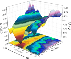
A Cu–Ni sectioned cathode made up of two hemicycles of each of the metals was used for reactive co-sputtering of a thin film combinatorial library of Cu–Ni oxides covering a total compositional spread of 63 at.%. The thickness profiling of the library showed a nonuniform film thickness with a maximum region shifted toward the Cu side of the cathode. The presence of CuO, Cu2O, NiO, and metallic Cu–Ni alloys was identified during the scanning x-ray diffraction investigations along the compositional spread. A distinct structural zone was defined between Cu–14 at.% Ni and Cu–19 at.% Ni, where the scanning electron microscopy investigations showed a higher surface porosity combined with smaller grain sizes. This zone corresponds to the maximum film thickness region and correlates well with the position of the maximum work function of the Cu–Ni oxide films as mapped using a scanning Kelvin probe. During local corrosion studies focused on Cu dissolution, an improved corrosion resistance was identified in the Ni rich side of the compositional spread.

Type
Articles
Copyright
Copyright © Materials Research Society 2013 

Access options

Get access to the full version of this content by using one of the access options below. (Log in options will check for institutional or personal access. Content may require purchase if you do not have access.)

References

REFERENCES

Monell, D.: Manufacture of Nickel-Copper Alloys. U.S. Patent No. 8 112 39, 1911.Google Scholar
Laughton, M.A. and Warne, D.F.: Electrical Engineer’s Reference Book, 6th ed. (Elsevier Science, Oxford, England, 2003), pp. 1043.Google Scholar
Schultze, J.W. and Hassel, A.W.: Passivity of metals, alloys, and semiconductors. In Encyclopedia of electrochemistry, Vol. 4. Corrosion and Oxide Films; Bard, A.J., Stratmann, M., and Frankel, G.S. (Wiley-VCH, Weinheim, Germany, 2007); pp. 216-280 & pp. 188-189.Google Scholar
Hashimoto, K., Yamasaki, M., Meguro, S., Sasaki, T., Katagiri, H., Izumiya, K., Kumagai, N., Habazaki, H., Akiyama, E., and Asami, K.: Materials for global carbon dioxide recycling. Corros. Sci. 44, 371 (2002).CrossRefGoogle Scholar
Miyauchi, M., Nakajima, A., Watanabe, T., and Hashimoto, K.: Photocatalysis and photoinduced hydrophilicity of various metal oxide thin films. Chem. Mater. 14, 2812 (2002).CrossRefGoogle Scholar
Hotovy, I., Huran, J., Janik, J., and Kobzev, A.B.: Deposition and properties of nickel oxide films produced by DC reactive magnetron sputtering. Vacuum 51, 157 (1998).CrossRefGoogle Scholar
Hotovy, I., Buc, D., Hascik, S., and Nennewitz, O.: Characterization of NiO thin films deposited by reactive sputtering. Vacuum 50, 41 (1998).CrossRefGoogle Scholar
Chen, H-L. and Yang, Y-S.: Effect of crystallographic orientations on electrical properties of sputter-deposited nickel oxide thin films. Thin Solid Films 516, 5590 (2008).CrossRefGoogle Scholar
Yang, J-L., Lai, Y-S., and Chen, J.S.: Effect of heat treatment on the properties of non-stoichiometric p-type nickel oxide films deposited by reactive sputtering. Thin Solid Films 488, 242 (2005).CrossRefGoogle Scholar
Karpinski, A., Ferrec, A., Richard-Plouet, M., Cattin, L., Djouadi, M.A., Brohan, L., and Jouan, P-Y.: Deposition of nickel oxide by direct current reactive sputtering effect of oxygen partial pressure. Thin Solid Films 520, 3609 (2012).CrossRefGoogle Scholar
Courtade, L., Turquat, C., Muller, C., Lisoni, J.G., Goux, L., Wouters, D.J., Goguenheim, D., Roussel, P., and Ortega, L.: Oxidation kinetics of Ni metallic films- formation of NiO-based resistive switching structures. Thin Solid Films 516, 4083 (2008).CrossRefGoogle Scholar
Otsuka, S., Furuya, S., Takeda, R., Shimizu, T., Shingubara, S., Watanabe, T., Takano, Y., and Takase, K.: Resistive switching characteristics of NiO/Ni nanostructure. Microelectron. Eng. 98, 367 (2012).CrossRefGoogle Scholar
Lee, C.B., Kang, B.S., Benayad, A., Lee, M.J., Ahn, S-E., Kim, K.H., Stefanovic, G., Park, Y., and Yoo, I.K.: Effects of metal electrodes on the resistive memory switching property of NiO thin films. Appl. Phys. Lett. 93, 042115 (2008).CrossRefGoogle Scholar
Song, X., Gao, L., and Mathur, S.: Synthesis, characterization, and gas sensing properties of porous nickel oxide nanotubes. J. Phys. Chem. C 115, 21730 (2011).CrossRefGoogle Scholar
Nancheva, N., Docheva, P., and Misheva, M.: Defects in Cu and Cu–O films produced by reactive magnetron sputtering. Mater. Lett. 39, 81 (1999).CrossRefGoogle Scholar
Chandra, R., Taneja, P., and Ayyub, P.: Optical properties of transparent nanocrystalline Cu2O thin films synthesized by high pressure gas sputtering. Nanostruct. Mater. 11, 505 (1999).CrossRefGoogle Scholar
Sivasankar Reddy, A., Uthanna, S., and Sreedhara Reddy, P.: Properties of dc magnetron sputtered Cu2O films prepared at different sputtering pressures. Appl. Surf. Sci. 253, 5287 (2007).CrossRefGoogle Scholar
Sivasankar Reddy, A., Venkata Rao, G., Uthanna, S., and Sreedhara Reddy, P.: Structural and optical studies on dc reactive magnetron sputtered Cu2O films. Mater. Lett. 60, 1617 (2006).CrossRefGoogle Scholar
Zhu, H., Zhang, J., Li, C., Pan, F., Wang, T., and Huang, B.: Cu2O thin films deposited by reactive direct current magnetron sputtering. Thin Solid Films 517, 5700 (2009).CrossRefGoogle Scholar
Hara, M., Kondo, T., Komoda, M., Ikeda, S., Shinohara, K., Tanaka, A., Kondoa, J.N., and Domen, K.: Cu2O as a photocatalyst for overall water splitting under visible light irradiation. Chem. Commun. (3), 357 (1998). doi: 10.1039/A707440I.CrossRefGoogle Scholar
Akimoto, K., Ishizuka, S., Yanagita, M, Nawa, Y, Paul, G.K., and Sakurai, T.: Thin film deposition of Cu2O and application for solar cells. Sol. Energy 80, 715 (2006).CrossRefGoogle Scholar
Yang, W-Y. and Rhee, S-W.: Effect of electrode material on the resistance switching of Cu2O films. Appl. Phys. Lett. 91, 232907 (2007).CrossRefGoogle Scholar
Miteva, V., Karpuzov, D., Ivanov, P., and Angelova, St.: Stoichiometry effects at Cu-Ni alloy surfaces during 5 keV Ar ion sputtering at room temperature. Nucl. Instrum. Methods Phys. Res., Sect. B 85, 340 (1994).CrossRefGoogle Scholar
Posadowski, W.M.: Self-sustained magnetron co-sputtering of Cu and Ni. Thin Solid Films 459, 258 (2004).CrossRefGoogle Scholar
Yang, M., Shi, Z., Feng, J., Pu, H., Li, G., Zhou, J., and Zhang, Q.: Copper doped nickel oxide transparent p-type conductive thin films deposited by pulsed plasma deposition. Thin Solid Films 519, 3021 (2011).CrossRefGoogle Scholar
Kikuchi, N., Tonooka, K., and Kusano, E.: Mechanisms of carrier generation and transport in Ni-doped Cu2O. Vacuum 80, 756 (2006).CrossRefGoogle Scholar
Burgstaller, W., Mardare, A.I., and Hassel, A.W.: Copper-zinc thin films reactively co-sputtered from a two-component sectioned cathode. Phys. Status Solidi A 210, 994 (2013).CrossRefGoogle Scholar
Voith, M., Luckeneder, G., and Hassel, A.W.: In situ identification and quantification in a flow cell with AAS downstream analytics. J. Sol. State Electrochem. 16, 3473 (2012).CrossRefGoogle Scholar
Wasa, K. and Hayakawa, S.: Handbook of Sputter Deposition Technology (Noyes Publications, Westwood, NJ, 2003), p. 57.Google Scholar
Ohring, M.: Materials Science of Thin Films, 2nd ed. (Academic Press, Waltham, MA, 2001), p. 176.Google Scholar
Thornton, J.A.: The microstructure of sputter-deposited coatings. J. Vac. Sci. Technol., A 4, 3056 (1986).CrossRefGoogle Scholar
Mardare, A.I., Yadav, A.P., Wieck, A.D., Stratmann, M., and Hassel, A.W.: Combinatorial electrochemistry on Al-Fe alloys. Sci. Technol. Adv. Mater. 9, 035009 (2008).CrossRefGoogle ScholarPubMed
Mardare, A.I., Ludwig, A., Savan, A., Wieck, A.D., and Hassel, A.W.: High-throughput study of the anodic oxidation of Hf-Ti thin films. Electrochim. Acta 54, 5171 (2009).CrossRefGoogle Scholar
Mardare, A.I., Savan, A., Ludwig, A., Wieck, A.D., and Hassel, A.W.: High-throughput synthesis and characterization of anodic oxides on Nb-Ti alloys. Electrochim. Acta 54, 5973 (2009).CrossRefGoogle Scholar
Mardare, A.I., Ludwig, A., Savan, A., Wieck, A.D., and Hassel, A.W.: Combinatorial investigation of Hf-Ta thin films and their anodic oxides. Electrochim. Acta 55, 7884 (2010).CrossRefGoogle Scholar
Atanasoski, R.T., Huang, S-M., Albani, O., and Orani, R.A.: A dry redox couple employed as the reference material in work function and corrosion potential measurements by the Kelvin technique. Corros. Sci. 36, 1513 (1994).CrossRefGoogle Scholar
Hansen, W.N. and Hansen, G.J.: Standard reference surfaces for work function measurements in air. Surf. Sci. 481, 172 (2001).CrossRefGoogle Scholar