Skip to main content Accessibility help
×
Hostname: page-component-586b7cd67f-t7fkt Total loading time: 0 Render date: 2024-11-20T12:21:35.995Z Has data issue: false hasContentIssue false

4 - Lightwaves in restricted geometries

from Part I - Basics

Published online by Cambridge University Press:  23 November 2018

Sergey V. Gaponenko
Affiliation:
National Academy of Sciences of Belarus
Hilmi Volkan Demir
Affiliation:
Nanyang Technological University, Singapore
Get access

Summary

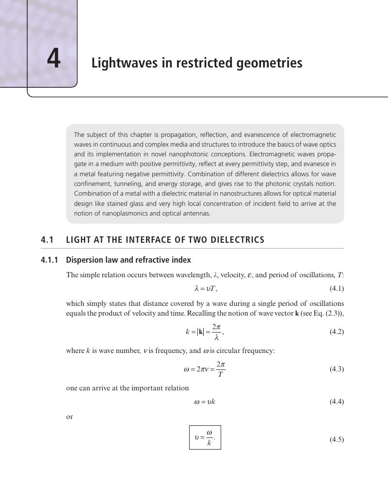
Image of the first page of this content. For PDF version, please use the ‘Save PDF’ preceeding this image.'
Type
Chapter
Information
Publisher: Cambridge University Press
Print publication year: 2018

Access options

Get access to the full version of this content by using one of the access options below. (Log in options will check for institutional or personal access. Content may require purchase if you do not have access.)

References

Further reading

Barber, E. M. (2008). Aperiodic Structures in Condensed Matter: Fundamentals and Applications. CRC Press.Google Scholar
Bharadwaj, P., Deutsch, B., and Novotny, L. (2009). Optical antennas. Adv Opt Photonics, 1(3), 438483.CrossRefGoogle Scholar
Born, M., and Wolf, E. (1999). Principles of Optics: Electromagnetic Theory of Propagation, Interference and Diffraction of Light. Cambridge University Press.Google Scholar
Dal Negro, L. (ed.) (2013). Optics of Aperiodic Structures: Fundamentals and Device Applications. CRC Press.Google Scholar
Joannopoulos, J. D., Johnson, S. G., Winn, J. N., and Meade, R. D. (2011). Photonic Crystals: Molding the Flow of Light. Princeton University Press.Google Scholar
Kavokin, A., Baumberg, J. J., Malpuech, G., and Laussy, F. P. (2007). Microcavities. Oxford University Press.Google Scholar
Krauss, T. F., and De La Rue, R. M. (1999). Photonic crystals in the optical regime: past, present and future. Progr Quant Electron, 23, 5196.CrossRefGoogle Scholar
Lagendijk, A., van Tiggelen, B., and Wiersma, D. S. (2009). Fifty years of Anderson localization. Phys Today, 62(8), 2429.Google Scholar
Lekner, J. (2016). Theory of Reflection: Reflection and Transmission of Electromagnetic, Particle and Acoustic Waves. Springer.Google Scholar
Li, J., Slandrino, A., and Engheta, N. (2007). Shaping light beams in the nanometer scale: a Yagi–Uda nanoantenna in the optical domain. Phys Rev B, 76, 25403.Google Scholar
Limonov, M. F., and De La Rue, R. M. (2012). Optical Properties of Photonic Structures: Interplay of Order and Disorder. CRC Press.Google Scholar
Lu, T., Peng, W., Zhu, S., and Zhang, D. (2016). Bio-inspired fabrication of stimuli-responsive photonic crystals with hierarchical structures and their applications. Nanotechnology, 27(12), 122001.Google Scholar
Maciá, E., (2005). The role of aperiodic order in science and technology. Rep Prog Phys, 69(2), 397.CrossRefGoogle Scholar
Novotny, L., and van Hulst, N. (2011). Antennas for light. Nat Photonics, 5(2), 8390.CrossRefGoogle Scholar
Park, Q. H., (2009). Optical antennas and plasmonics. Contemp Phys, 50(2), 407423.Google Scholar
Parker, A. R. (2000). 515 million years of structural color. J Optics A, 2, R15R28.Google Scholar
Poelwijk, F. J. (2000). Interference in Random Lasers. PhD thesis, University of Amsterdam.Google Scholar
Thompson, D. (2007). Michael Faraday’s recognition of ruby gold: the birth of modern nanotechnology. Gold Bulletin, 40(4), 267269.Google Scholar
Van den Broek, J. M., Woldering, L. A., Tjerkstra, R. W., et al. (2012). Inverse-woodpile photonic band gap crystals with a cubic diamond-like structure made from single-crystalline silicon. Adv Funct Mater, 22(1), 2531.CrossRefGoogle Scholar
Vukusic, P., and Sambles, J. (2003). Photonic structures in biology. Nature, 424, 852855.Google Scholar
Vukusic, P., Hallam, B., and Noyes, J. (2007). Brilliant whiteness in ultrathin beetle scales. Science, 315(5810), 348.CrossRefGoogle ScholarPubMed
Wilts, B. D., Michielsen, K., De Raedt, H., and Stavenga, D. G. (2012). Hemispherical Brillouin zone imaging of a diamond-type biological photonic crystal. J R Soc Interface, 9(72), 16091614.CrossRefGoogle ScholarPubMed

References

Abadeer, N. S., Brennan, M. R., Wilson, W. L., and Murphy, C. J. (2014). Distance and plasmon wavelength dependent fluorescence of molecules bound to silica-coated gold nanorods. ACS Nano, 8(8), 83928406.Google Scholar
Arnold, S., Khoshsima, M., Teraoka, I., Holler, S., and Vollmer, F. (2003). Shift of whispering-gallery modes in microspheres by protein adsorption. Opt Lett, 28(4), 272274.Google Scholar
Baldycheva, A., Tolmachev, V., Perova, T., et al. (2011). Silicon photonic crystal filter with ultrawide passband characteristics. Opt Lett, 36, 18541856.Google Scholar
Bendickson, J. M., Dowling, J. P., and Scalora, M. (1996). Analytic expressions for the electromagnetic mode density in finite, one-dimensional, photonic band-gap structures. Phys Rev E, 53, 41074121.Google Scholar
Birner, A., Wehrspohn, R. B., Gösele, U. M., and Busch, K. (2001). Silicon-based photonic crystals. Adv Mat, 13, 377382.Google Scholar
Bruggeman, D. A. G. (1935). Berechnung verschiedener physikalischer Konstanten von heterogenen Substanzen. I. Dielektrizitetskonstanten und Leitfehigkeiten der Mischkorper aus isotropen Substanzen. Ann Phys, 416, 636664.Google Scholar
Busch, K., von Freymann, G., Linden, S., et al. (2007). Periodic nanostructures for photonics. Phys Rep, 444, 101202.Google Scholar
Chen, Y. C., and Bahl, G. (2015). Raman cooling of solids through photonic density of states engineering. Optica, 2(10), 893899.Google Scholar
Chung, T., Lee, S. Y., Song, E. Y., Chun, H., and Lee, B. (2011). Plasmonic nanostructures for nano-scale bio-sensing. Sensors, 11(11), 1090710929.CrossRefGoogle ScholarPubMed
Domaradzki, J., Kaczmarek, D., Mazur, M., et al. (2016). Investigations of optical and surface properties of Ag single thin film coating as semitransparent heat reflective mirror. Mater Sci Poland, 34(4), 747753.Google Scholar
Gaponenko, S. V. (2010). Introduction to Nanophotonics. Cambridge University Press.Google Scholar
Ghenuche, P., Cherukulappurath, S., Taminiau, T. H., van Hulst, N. F., and Quidant, R. (2008). Spectroscopic mode mapping of resonant plasmon nanoantennas. Phys Rev Lett, 101(11), 116805.Google Scholar
Guzatov, D. V., and Klimov, V. V. (2011). Optical properties of a plasmonic nano-antenna: an analytical approach. New J Phys, 13(5), 053034.Google Scholar
Ho, K. M., Chan, C. T., Soukoulis, C. M., Biswas, R., and Sigalas, M. (1994). Photonic band gaps in three dimensions: new layer-by-layer periodic structures. Solid State Commun, 89(5), 413416.Google Scholar
Joannopoulos, J. D., Johnson, S. G., Winn, J. N., and Meade, R. D. (2011). Photonic Crystals: Molding the Flow of Light. Princeton University Press.Google Scholar
Kreibig, U., and Vollmer, M. (1995). Optical Properties of Metal Clusters. Springer.CrossRefGoogle Scholar
Li, K., Stockman, M. I., and Bergman, D. J. (2003). Self-similar chain of metal nanospheres as an efficient nanolens. Phys Rev Lett, 91(22), 227402.Google Scholar
Lin, S.-Y., Fleming, J. G., Hetherington, D. L., et al. (1998). A three-dimensional photonic crystal operating at infrared wavelengths. Nature, 394(6690), 251253.Google Scholar
Lutich, A. A., Gaponenko, S. V., Gaponenko, N. V., et al. (2004). Anisotropic light scattering in nanoporous materials: a photon density of states effect. Nano Lett, 4, 17551758.Google Scholar
Madelung, O. (2012). Semiconductors: Data Handbook. Springer Science & Business Media.Google Scholar
Pellegrini, V., Tredicucci, A., Mazzoleni, C., and Pavesi, L. (1995). Enhanced optical properties in porous silicon microcavities. Phys Rev B, 52, R14328–R14331.Google Scholar
Petrov, E. P., Bogomolov, V. N., Kalosha, I. I., and Gaponenko, S. V. (1998). Spontaneous emission of organic molecules in a photonic crystal. Phys Rev Lett, 81, 7780.Google Scholar
Reynolds, A., Lopez-Tejeira, F., Cassagne, D., et al. (1999). Spectral properties of opal-based photonic crystals having a SiO2 matrix. Phys Rev B, 60, 1142211426.Google Scholar
Sakoda, K. (2004). Optical Properties of Photonic Crystals. Springer.Google Scholar
Schuck, P. J., Fromm, D. P., Sundaramurthy, A., Kino, G. S., and Moerner, W. E. (2005). Improving the mismatch between light and nanoscale objects with gold bowtie nanoantennas. Phys Rev Lett, 94(1), 017402.Google Scholar
Schuurmans, F. J. P., Vanmaekelbergh, D., van de Lagemaat, J., and Lagendijk, A. (1999). Strongly photonic macroporous gallium phosphide networks. Science, 284, 141143.Google Scholar
Strutt, J. W. (Lord Rayleigh) (1887). On the maintenance of vibrations by forces of double frequency, and on the propagation of waves through a medium endowed with a periodic structure. Phil Mag S, 24, 145159.Google Scholar
Taminiau, T. H., Stefani, F. D., and van Hulst, N. F. (2008). Enhanced directional excitation and emission of single emitters by a nano-optical Yagi–Uda antenna. Opt Expr, 16 (14), 1085810866.Google Scholar
Teyssier, J., Saenko, S. V., Van Der Marel, D., and Milinkovitch, M. C. (2015). Photonic crystals cause active colour change in chameleons. Nat Commun, 6, 6368.Google Scholar
Tjerkstra, R. W., Woldering, L. A., van den Broek, J. M., et al. (2011). Method to pattern etch masks in two inclined planes for three-dimensional nano-and microfabrication. J Vac Sci Technol, 29(6), 061604.Google Scholar
Vlasov, Y. A., Bo, X. Z., Sturm, J. C., and Norris, D. J. (2001). On-chip natural assembly of silicon photonic band gap crystals. Nature, 414, 289293.Google Scholar
Voitovich, A. P. (2006). Spectral properties of films. In: Di Bartolo, B. and Forte, O. (eds.), Advance in Spectroscopy for Lasers and Sensing. Springer, 351353.Google Scholar
Vukusic, P., and Sambles, J. (2003). Photonic structures in biology. Nature, 424, 852855.Google Scholar
Wang, R., Wang, X., -H., Gu, B., -Y., and Yang, G., -Z. (2001). Effects of shapes and orientations of scatterers and lattice symmetries on the photonic band gap in two-dimensional photonic crystals. J Appl Phys, 90, 43074312.CrossRefGoogle Scholar
Yariv, A., and Yeh, P. (1984). Optical Waves in Crystals. Wiley & Sons.Google Scholar

Save book to Kindle

To save this book to your Kindle, first ensure [email protected] is added to your Approved Personal Document E-mail List under your Personal Document Settings on the Manage Your Content and Devices page of your Amazon account. Then enter the ‘name’ part of your Kindle email address below. Find out more about saving to your Kindle.

Note you can select to save to either the @free.kindle.com or @kindle.com variations. ‘@free.kindle.com’ emails are free but can only be saved to your device when it is connected to wi-fi. ‘@kindle.com’ emails can be delivered even when you are not connected to wi-fi, but note that service fees apply.

Find out more about the Kindle Personal Document Service.

Available formats
×

Save book to Dropbox

To save content items to your account, please confirm that you agree to abide by our usage policies. If this is the first time you use this feature, you will be asked to authorise Cambridge Core to connect with your account. Find out more about saving content to Dropbox.

Available formats
×

Save book to Google Drive

To save content items to your account, please confirm that you agree to abide by our usage policies. If this is the first time you use this feature, you will be asked to authorise Cambridge Core to connect with your account. Find out more about saving content to Google Drive.

Available formats
×