Hostname: page-component-586b7cd67f-r5fsc Total loading time: 0 Render date: 2024-11-28T14:53:31.714Z Has data issue: false hasContentIssue false

Three-Dimensional Point Defect Imaging by Large-angle Illumination STEM

Published online by Cambridge University Press:  04 August 2017

Ryo Ishikawa
Affiliation:
Institute of Engineering Innovation, University of Tokyo, Bunkyo, Tokyo 113-8656, Japan
Stephen J. Pennycook
Affiliation:
Department of Materials Science & Engineering, National University of Singapore, 177576, Singapore
Andrew R. Lupini
Affiliation:
Materials Science and Technology Division, Oak Ridge National Laboratory, TN, 377831, USA
Scott D. Findlay
Affiliation:
School of Physics and Astronomy, Monash University, Victoria 3800, Australia
Naoya Shibata
Affiliation:
Institute of Engineering Innovation, University of Tokyo, Bunkyo, Tokyo 113-8656, Japan Nanostructures Research Laboratory, Japan Fine Ceramics Center, Nagoya, Aichi 456-8587, Japan
Yuichi Ikuhara
Affiliation:
Institute of Engineering Innovation, University of Tokyo, Bunkyo, Tokyo 113-8656, Japan Nanostructures Research Laboratory, Japan Fine Ceramics Center, Nagoya, Aichi 456-8587, Japan

Abstract

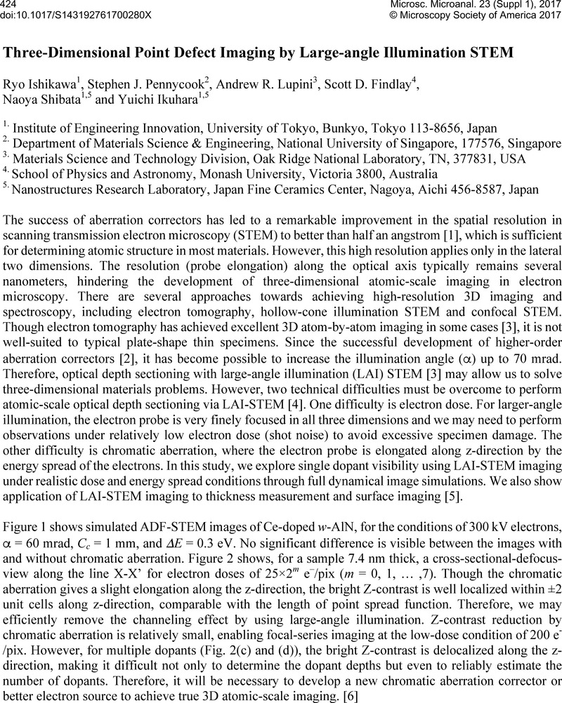
Image of the first page of this content. For PDF version, please use the ‘Save PDF’ preceeding this image.'
Type
Abstract
Copyright
© Microscopy Society of America 2017 

References

[1] Sawada, H., et al, Microscopy 64 2015 213.Google Scholar
[2] Sawada, H., et al, J. Electron Microscopy 58 2009 341.CrossRefGoogle Scholar
[3] Yang, Y., et al, Nature 542 2017 75.Google Scholar
[4] Ishikawa, R., et al, Ultramicroscopy 151 2015 122.Google Scholar
[5] Ishikawa, R., et al, Appl. Phys. Lett 109 2016 163102.Google Scholar
[6] A part of this work was supported by the Research & Development Initiative for Scientific Innovation of New Generation Batteries II (RISING II). A.R.L. was supported by the Office of Basic Energy Sciences, Materials Sciences and Engineering Division, U.S. Department of Energy.Google Scholar