Hostname: page-component-586b7cd67f-rdxmf Total loading time: 0 Render date: 2024-11-25T13:34:55.923Z Has data issue: false hasContentIssue false

Defect Imaging and Structure Evolution in GST Films During In-situ Heating

Published online by Cambridge University Press:  30 July 2020

Chanchal Ghosh
Affiliation:
Department of Electrical & Computer Engineering, University of Connecticut, Storrs, Connecticut, United States
Manish Singh
Affiliation:
Department of Electrical & Computer Engineering, University of Connecticut, Storrs, Connecticut, United States
John Watt
Affiliation:
Center for Integrated Nanotechnologies, Los Alamos, New Mexico, United States
Helena Silva
Affiliation:
Department of Electrical & Computer Engineering, University of Connecticut, Storrs, Connecticut, United States
C Barry Carter
Affiliation:
Department of Chemical & Biomolecular Engineering, University of Connecticut, Storrs, CT, United States Center of Integrated Nanotechnologies, Sandia National Laboratories, Albuquerque, NM, USA

Abstract

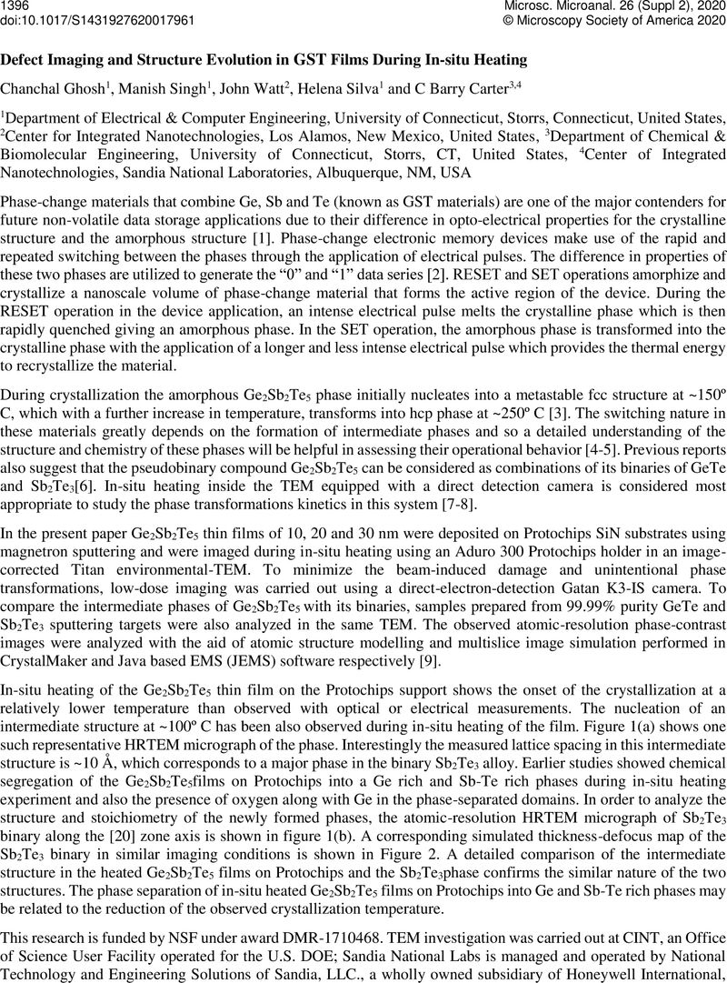
Image of the first page of this content. For PDF version, please use the ‘Save PDF’ preceeding this image.'
Type
Advances in Electron Microscopy to Characterize Materials Embedded in Devices
Copyright
Copyright © Microscopy Society of America 2020

References

Hegedus, J, Elliott, SR (2008) Microscopic origin of the fast crystallization ability of Ge-Sb-Te phase-change memory materials. Nature Materials 7(5), 39940510.1038/nmat2157CrossRefGoogle ScholarPubMed
Friedrich, I, Weidenhof, V, Njoroge, W, Franz, P, Wuttig, M (2000) Structural transformations of Ge2Sb2Te5 films studied by electrical resistance measurements. Journal of Applied Physics 87, 4130413410.1063/1.373041CrossRefGoogle Scholar
Tripathi, S, Janish, M, Dirisaglik, F, Cywar, A, Zhu, Y, Jungjohann, K, Silva, H, Carter, CB (2018) Phase-Change Materials; the Challenges for TEM. Microscopy and Microanalysis 24, S1, 1904–05.10.1017/S1431927618010000CrossRefGoogle Scholar
Lazzarini, L, Rotunno, E (2017) Crystal structure assessment of Ge-Sb-Te nanowires. Materials Science in Semiconductor Processing 65, 778710.1016/j.mssp.2016.07.008CrossRefGoogle Scholar
Lotnyk, A, Bernutz, S, Sun, X et al. (2016) Real-space imaging of atomic arrangement and vacancy layers ordering in laser crystallised Ge2Sb2Te5 phase change thin films. Acta Materialia 105, 1810.1016/j.actamat.2015.12.010CrossRefGoogle Scholar
Zheng, Y, Xia, M, Cheng, Y et al. (2016) Direct observation of metastable face centered cubic Sb2Te3 crystal. Nano Research 9(11), 3453346210.1007/s12274-016-1221-8CrossRefGoogle Scholar
Williams, DB, Carter, CB (2009) Transmission electron microscopy- A textbook for materials science, 2nd Ed. Springer, New York10.1007/978-0-387-76501-3CrossRefGoogle Scholar
Carter, CB, Williams, DB (Eds.) (2016) Transmission electron microscopy: diffraction, imaging and spectrometry, Springer, Berlin Heidelberg, 178010.1007/978-3-319-26651-0CrossRefGoogle Scholar
Stadelmann, P (1987) EMS – a software package for electron diffraction analysis and HREM image simulation in materials science, Ultramicroscopy 21(2), 13114510.1016/0304-3991(87)90080-5CrossRefGoogle Scholar