Hostname: page-component-586b7cd67f-t7czq Total loading time: 0 Render date: 2024-12-01T01:26:53.302Z Has data issue: false hasContentIssue false

CVD Diamond Films - Synthesis, Microstructure, Applications

Published online by Cambridge University Press:  04 August 2017

Wolfgang Jaeger*
Affiliation:
Institute for Materials Science, Christian Albrechts University Kiel, DE 24143 Kiel, Germany

Abstract

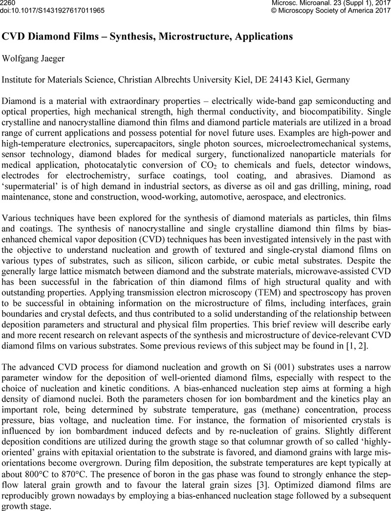
Image of the first page of this content. For PDF version, please use the ‘Save PDF’ preceeding this image.'
Type
Abstract
Copyright
© Microscopy Society of America 2017 

References

Selected References

[1] Nebel, C E, et al(eds) Thin Film Diamond. Elsevier Vol. 76 2003.Google Scholar
[2] Srikanth, V. & Jiang, X. (2011). Synthetic Diamond Films: Preparation, Electrochemistry, Characterization, and Applications (eds E. Brillas & C. A. Martinez-HuitleJohn Wiley Hoboken, USA.Google Scholar
[3] Jiang, X., Schiffmann, K., Klages, C.-P, Wittorf, D., Jia, C. L., Urban, K. & Jäger, W. J. Appl. Phys 83 1998). p 2511.Google Scholar
[4] Jäger, W., Wittorf, D., Jia, C. L. & Urban, K. Advances in Science and Technology 21 1999). p 137.Google Scholar
[5] Bauer, T., et al, Diamond & Related Materials 14 2005). p 314.Google Scholar
[6] Wittorf, D., Jäger, W., Dieker, C., Flöter, A. & Güttler, H. Diamond and Related Mat 9 2000 1696.Google Scholar
[7] Jiang, X. & Jia, C.L. Phys. Rev. Lett 84 2000). p 3658.Google Scholar
[8] Neethling, J., et al, Diamond & Related Materials 49 2014). p 1.Google Scholar
[9] Turner, S., et al, Nanoscale 8 2016). p 2212.Google Scholar
[10] Williams, O. A., Hees, J., Dieker, Ch., Jäger, W., Kirste, L. & Nebel, C.E. ACS NANO 4 2010 4824.Google Scholar
[11] Barroo, C, Magyar, A, Akey, A & Bell, D C Microscopy & Microanalysis 22(S3 2016). p. 694.CrossRefGoogle Scholar