Hostname: page-component-586b7cd67f-dsjbd Total loading time: 0 Render date: 2024-11-24T14:04:32.436Z Has data issue: false hasContentIssue false

The Combination of STEM Tomography and STEM/EDS Analysis of NiSi Formation Related Defects in Semiconductor Wafer-foundries

Published online by Cambridge University Press:  25 July 2016

B. Fu
Affiliation:
GLOBALFOUNDRIES, 400 Stone Break Rd Extension, Malta, NY, USA
M. Gribelyuk
Affiliation:
GLOBALFOUNDRIES, 400 Stone Break Rd Extension, Malta, NY, USA
L. Dumas
Affiliation:
GLOBALFOUNDRIES, 400 Stone Break Rd Extension, Malta, NY, USA
C. Fang
Affiliation:
GLOBALFOUNDRIES, 400 Stone Break Rd Extension, Malta, NY, USA
N. LaManque
Affiliation:
GLOBALFOUNDRIES, 400 Stone Break Rd Extension, Malta, NY, USA
L. Hodgkins
Affiliation:
GLOBALFOUNDRIES, 400 Stone Break Rd Extension, Malta, NY, USA
E. Chen
Affiliation:
GLOBALFOUNDRIES, 400 Stone Break Rd Extension, Malta, NY, USA

Abstract

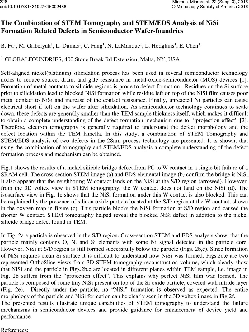
Image of the first page of this content. For PDF version, please use the ‘Save PDF’ preceeding this image.'
Type
Abstract
Copyright
© Microscopy Society of America 2016 

References

[1] Deng, F., et al, J. Appl. Phys. 81 (1997). p. 8047.CrossRefGoogle Scholar
[2] Zhao, W., et al, Microsc. Microanal. 20 (2014). p. 362.CrossRefGoogle Scholar