Hostname: page-component-cd9895bd7-dk4vv Total loading time: 0 Render date: 2025-01-05T04:08:31.156Z Has data issue: false hasContentIssue false

Analyses of Interfaces in Wafer-Bonded Tandem Solar Cells by Aberration-Corrected STEM and EELS

Published online by Cambridge University Press:  27 August 2014

Dietrich Häussler
Affiliation:
Institute for Materials Science, Christian Albrechts University Kiel, Kaiserstraße 2, 24143 Kiel, Germany
Lothar Houben
Affiliation:
Ernst Ruska Centre for Microscopy and Spectroscopy with Electrons, Research Centre Juelich GmbH, 52425 Juelich, Germany
Rafal E. Dunin-Borkowski
Affiliation:
Ernst Ruska Centre for Microscopy and Spectroscopy with Electrons, Research Centre Juelich GmbH, 52425 Juelich, Germany
Stephanie Essig
Affiliation:
Fraunhofer Institute for Solar Energy Systems ISE, Heidenhofstraße 2, 79110 Freiburg, Germany
Frank Dimroth
Affiliation:
Fraunhofer Institute for Solar Energy Systems ISE, Heidenhofstraße 2, 79110 Freiburg, Germany
Wolfgang Jäger
Affiliation:
Institute for Materials Science, Christian Albrechts University Kiel, Kaiserstraße 2, 24143 Kiel, Germany

Abstract

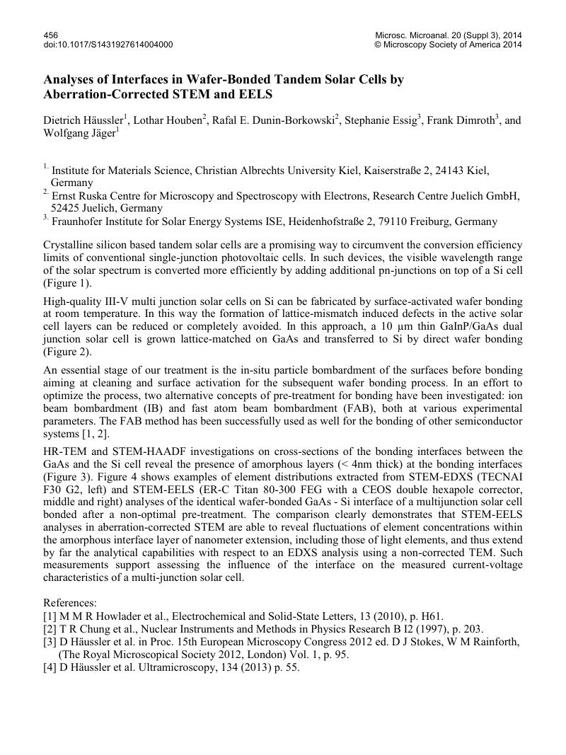
Image of the first page of this content. For PDF version, please use the ‘Save PDF’ preceeding this image.'
Type
Abstract
Copyright
Copyright © Microscopy Society of America 2014 

References

[1] Howlader, M M R, et al., Electrochemical and Solid-State Letters, 13 (2010), p. H61.Google Scholar
[2] Chung, T R, et al., Nuclear Instruments and Methods in Physics Research B I2 (1997), p. 203.Google Scholar
[3] Häussler, D, et al., in Proc. 15th European Microscopy Congress (2012). ed. D J Stokes, W M Rainforth, The Royal Microscopical Society (2012, London) Vol. 1, p. 95.Google Scholar
[4] Häussler, D, et al., Ultramicroscopy, 134 (2013) p. 55.Google Scholar