Hostname: page-component-78c5997874-94fs2 Total loading time: 0 Render date: 2024-11-15T07:29:56.430Z Has data issue: false hasContentIssue false

Platinum metallization on silicon and silicates

Published online by Cambridge University Press:  18 November 2020

Jeffrey C. Taylor*
Affiliation:
Department of Applied Physics and Applied Mathematics, Columbia University, New York, New York, USA
*
Get access

Abstract

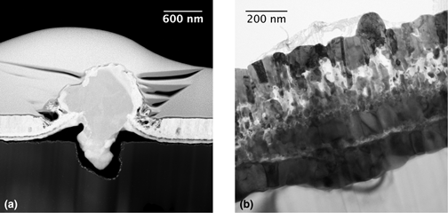
Thin films of platinum deposited by physical vapor deposition (PVD) processes such as evaporation and sputtering are used in many academic and industrial settings, for example to provide metallization when tolerance to corrosive thermal cycling is desired, or in electrocatalysis research. In this review, various practical considerations for platinum (Pt) metallization on both Si and SiO2 are placed in context with a comprehensive data review of diffusion measurements. The relevance of diffusion phenomena to the development of microstructure during deposition as well as the effect of microstructure on the properties of deposited films are discussed with respect to the Pt–Si system. Since Pt and Si readily form silicides, diffusion barriers are essential components of Pt metallization on Si, and various failure modes for diffusion barriers between Pt and Si are clarified with images obtained by electron microscopy. Adhesion layers for Pt films deposited on SiO2 are also considered.

Type
REVIEW
Copyright
Copyright © The Author(s), 2020, published on behalf of Materials Research Society by Cambridge University Press

Access options

Get access to the full version of this content by using one of the access options below. (Log in options will check for institutional or personal access. Content may require purchase if you do not have access.)

Footnotes

b)

Present address: Sandia National Laboratories, Albuquerque, New Mexico, USA.

References

Beard, B.C. and Ross, P.N.: Characterization of a titanium-promoted supported platinum electrocatalyst. J. Electrochem. Soc. 133, 18391845 (1986).10.1149/1.2109033CrossRefGoogle Scholar
Smithells, C.J.: Smithells Metals Reference Book [Electronic Resource] (Elsevier Butterworth-Heinemann, Boston, MA, USA, 2004).Google Scholar
Mantese, J.V. and Alcini, W.V.: Platinum wire wedge bonding: A new IC and microsensor interconnect. J. Electron. Mater. 17, 285289 (1988).10.1007/BF02652107CrossRefGoogle Scholar
Robinson, J.E., Labrador, N.Y., Chen, H., Sartor, B.E., and Esposito, D.V.: Silicon oxide-encapsulated platinum thin films as highly active electrocatalysts for carbon monoxide and methanol oxidation. ACS Catal. 8, 1142311434 (2018).10.1021/acscatal.8b03626CrossRefGoogle Scholar
Zeiser, R., Wagner, P., and Wilde, J.: Investigation of ultrasonic platinum and palladium wire bonding as interconnection technology for high-temperature SiC-MEMS. In 2012 4th Electronic System-Integration Technology Conference, 2012; pp. 1–6. doi:10.1109/ESTC.2012.6542125.CrossRefGoogle Scholar
Brachmann, E., Seifert, M., Ernst, D., Menzel, S.B., and Gemming, T.: Pt-wire bonding optimization for electroplated Pt films on γ-Al2O3 for high temperature and harsh environment applications. Sens. Actuators Phys. 284, 129134 (2018).10.1016/j.sna.2018.10.023CrossRefGoogle Scholar
Ohring, M.: Materials Science of Thin Films (Elsevier Science & Technology, Burlington, MA, USA, 2001).Google Scholar
Mahan, J.E.: Physical Vapor Deposition of Thin Films (Wiley, Chichester, U.K., 2000).Google Scholar
Maissel, L.I. and Glang, R., eds: Handbook of Thin Film Technology (McGraw-Hill, New York, NY, USA, 1970).Google Scholar
Sze, S.M.: Physics of Semiconductor Devices (Wiley, New York, NY, USA, 1981).Google Scholar
Tu, K.N., Mayer, J.W., and Feldman, L.C.: Electronic Thin Film Science: For Electrical Engineers and Materials Scientists (Maxwell Macmillan International, Toronto, Canada, 1992).Google Scholar
Derrien, J.: 4.2 Schottky barrier heights of TM silicides on Si and GaAs. In Properties of Metal Silicides, Maex, K. and Van Rossum, M., eds. (INSPEC, London, U.K., 1995), pp. 164168.Google Scholar
Solina, D.M., Cheary, R.W., Swift, P.D., Dligatch, S., McCredie, G.M., Gong, B., and Lynch, P.: Investigation of the interfacial structure of ultra-thin platinum films using X-ray reflectivity and X-ray photoelectron spectroscopy. Thin Solid Films 372, 94103 (2000).10.1016/S0040-6090(00)01044-0CrossRefGoogle Scholar
Gas, P. and d'Heurle, F.M.: 4 Diffusion in silicides. In Diffusion in Semiconductors, Beke, D.L., ed.; Landolt-Börnstein - Group III Condensed Matter (Springer, Berlin, Heidelberg, Germany, 1998); pp. 138. doi:10.1007/10426818_13.Google Scholar
Pretorius, R., Harris, J.M., and Nicolet, M.-A.: Reaction of thin metal films with SiO2 substrates. Solid-State Electron 21, 667675 (1978).10.1016/0038-1101(78)90335-0CrossRefGoogle Scholar
Mohr, P.J., Newell, D.B., and Taylor, B.N.: CODATA recommended values of the fundamental physical constants: 2014. Rev. Mod. Phys. 88, 035009 (2016).10.1103/RevModPhys.88.035009CrossRefGoogle Scholar
Liempt, J.A.M.v.: Die Berechnung der Auflockerungswärme der Metalle aus Rekristallisationsdaten. Z. Für Phys. 96, 534541 (1935).10.1007/BF01337708CrossRefGoogle Scholar
Gjostein, N.A.: 9 Short circuit diffusion. In Diffusion; Papers Presented at a Seminar of the American Society for Metals, October 14 and 15, 1972. (American Society for Metals: Metals Park, OH, USA, 1973).Google Scholar
Brown, A.M. and Ashby, M.F.: Correlations for diffusion constants. Acta Metall. 28, 10851101 (1980).10.1016/0001-6160(80)90092-9CrossRefGoogle Scholar
Balluffi, R.W., Allen, S.M., and Carter, W.C.: Kinetics of Materials (Wiley-Interscience, Hoboken, NJ, USA, 2005).10.1002/0471749311CrossRefGoogle Scholar
Flynn, C.P.: Point Defects and Diffusion (Clarendon Press, Oxford, U.K., 1972).Google Scholar
Balluffi, R.W. and Blakely, J.M.: Special aspects of diffusion in thin films. Thin Solid Films 25, 363392 (1975).10.1016/0040-6090(75)90056-5CrossRefGoogle Scholar
Bocquet, J.L., Brebec, G., and Limoge, Y.: 7 Diffusion in metals and alloys. In Physical Metallurgy, 4th ed., Cahn, R.W. and Haasen, P., eds. (Elsevier B.V., North-Holland, Oxford, U.K., 1996); pp. 535668.10.1016/B978-044489875-3/50012-0CrossRefGoogle Scholar
Murarka, S.: 5 Diffusion barriers in semiconductor devices/circuits .In Diffusion Processes in Advanced Technological Materials, Gupta, Devendra, ed. (William Andrew, Inc., Norwich, NY, USA, 2005), pp. 239281.Google Scholar
Cattaneo, F., Germagnoli, E., and Grasso, F.: Self-diffusion in platinum. Philos. Mag. J. Theor. Exp. Appl. Phys. 7, 13731383 (1962).Google Scholar
Maier, K., Mehrer, H., Lessmann, E., and Schüle, W.: Self-diffusion in nickel at low temperatures. Phys. Status Solidi B 78, 689698 (1976).10.1002/pssb.2220780230CrossRefGoogle Scholar
Flynn, C.P.: Constraints on the growth of metallic superlattices. J. Phys. F Met. Phys. 18, L195 (1988).10.1088/0305-4608/18/9/005CrossRefGoogle Scholar
Lazarus, D.: Diffusion in metals. In Solid State Physics, Seitz, F. and Turnbull, D., eds., Vol. 10 (Academic Press, 1960); pp. 71126. doi:10.1016/S0081-1947(08)60701-8.Google Scholar
Kidson, G.V. and Ross, R.: Self diffusion in polycrystalline platinum. Int. J. Appl. Radiat. Isot. 2, 261 (1957).10.1016/0020-708X(57)90259-4CrossRefGoogle Scholar
Schumacher, D., Seeger, A., and Härlin, O.: Vacancies, divacancies, and self-diffusion in platinum. Phys. Status Solidi B 25, 359371 (1968).10.1002/pssb.19680250135CrossRefGoogle Scholar
Seeger, A. and Chik, K.P.: Diffusion mechanisms and point defects in silicon and germanium. Phys. Status Solidi B 29, 455542 (1968).10.1002/pssb.19680290202CrossRefGoogle Scholar
Million, B. and Kucera, J.: Diffusion of sup(193 m)Pt in platinum, γ-iron, cobalt and nickel. Kov. Mater. 11, 300306 (1973).Google Scholar
Rein, G., Mehrer, H., and Maier, K.: Diffusion of 197Pt and 199Au in platinum at low temperatures. Phys. Status Solidi A 45, 253261 (1978).10.1002/pssa.2210450130CrossRefGoogle Scholar
Nachtrieb, N.H., Weil, J.A., Catalano, E., and Lawson, A.W.: Self-diffusion in solid sodium. II. The effect of pressure. J. Chem. Phys. 20, 11891194 (1952).10.1063/1.1700709CrossRefGoogle Scholar
Nachtrieb, N.H. and Handler, G.S.: A relaxed vacancy model for diffusion in crystalline metals. Acta Metall. 2, 797802 (1954).10.1016/0001-6160(54)90031-0CrossRefGoogle Scholar
Neumann, G.: Diffusion mechanisms in metals. In Defect and Diffusion Forum, Murch, G.E. and Fischer, D.J., eds.; Defect and Diffusion Forum, Vols. 66–69 (Sci-Tech Publications, Brookfield, VT, USA, 1990); pp. 4364. doi: 10.4028/www.scientific.net/DDF.66-69.43.Google Scholar
Peterson, N.L.: Self-diffusion in pure metals. J. Nucl. Mater. 69–70, 337 (1978).10.1016/0022-3115(78)90234-9CrossRefGoogle Scholar
Frank, W., Gösele, U., Mehrer, H., and Seeger, A.: 2-Diffusion in silicon and germanium. In Diffusion in Crystalline Solids, Murch, G.E. and Nowick, A.S., eds. (Academic Press, 1984); pp. 63142. doi:10.1016/B978-0-12-522662-2.50007-8.CrossRefGoogle Scholar
Bracht, H., Haller, E.E., and Clark-Phelps, R.: Silicon self-diffusion in isotope heterostructures. Phys. Rev. Lett. 81, 393396 (1998).10.1103/PhysRevLett.81.393CrossRefGoogle Scholar
Bracht, H., Stolwijk, N.A., and Mehrer, H.: Properties of intrinsic point defects in silicon determined by zinc diffusion experiments under nonequilibrium conditions. Phys. Rev. B 52, 1654216560 (1995).10.1103/PhysRevB.52.16542CrossRefGoogle ScholarPubMed
Ural, A., Griffin, P.B., and Plummer, J.D.: Fractional contributions of microscopic diffusion mechanisms for common dopants and self-diffusion in silicon. J. Appl. Phys. 85, 64406446 (1999).10.1063/1.370285CrossRefGoogle Scholar
Morehead, F.F.: The diffusivity of self-interstitials in silicon. MRS Online Proc. Libr. Arch. 104, 99104 (1987).10.1557/PROC-104-99CrossRefGoogle Scholar
Frank, F.C. and Turnbull, D.: Mechanism of diffusion of copper in germanium. Phys. Rev. 104, 617618 (1956).10.1103/PhysRev.104.617CrossRefGoogle Scholar
Gösele, U., Frank, W., and Seeger, A.: Mechanism and kinetics of the diffusion of gold in silicon. Appl. Phys. 23, 361368 (1980).10.1007/BF00903217CrossRefGoogle Scholar
Jacob, M., Pichler, P., Ryssel, H., and Falster, R.: Determination of vacancy concentrations in the bulk of silicon wafers by platinum diffusion experiments. J. Appl. Phys. 82, 182191 (1997).10.1063/1.365796CrossRefGoogle Scholar
Zimmermann, H. and Ryssel, H.: The modeling of platinum diffusion in silicon under non-equilibrium conditions. J. Electrochem. Soc. 139, 256262 (1992).10.1149/1.2069180CrossRefGoogle Scholar
Lerch, W., Stolwijk, N.A., Mehrer, H., and Poisson, C.: Diffusion of platinum into dislocated and non-dislocated silicon. Semicond. Sci. Technol. 10, 1257 (1995).10.1088/0268-1242/10/9/009CrossRefGoogle Scholar
Badr, E., Pichler, P., and Schmidt, G.: Modeling platinum diffusion in silicon. J. Appl. Phys. 116, 133508 (2014).10.1063/1.4896909CrossRefGoogle Scholar
Mantovani, S., Nava, F., Nobili, C., and Ottaviani, G.: In-diffusion of Pt in Si from the PtSi/Si interface. Phys. Rev. B 33, 55365544 (1986).10.1103/PhysRevB.33.5536CrossRefGoogle Scholar
Morehead, F., Stolwijk, N.A., Meyberg, W., and Gösele, U.: Self-interstitial and vacancy contributions to silicon self-diffusion determined from the diffusion of gold in silicon. Appl. Phys. Lett. 42, 690692 (1983).10.1063/1.94074CrossRefGoogle Scholar
Fahey, P.M., Griffin, P.B., and Plummer, J.D.: Point defects and dopant diffusion in silicon. Rev. Mod. Phys. 61, 289384 (1989).10.1103/RevModPhys.61.289CrossRefGoogle Scholar
Simmons, R.O. and Balluffi, R.W.: Measurements of equilibrium vacancy concentrations in aluminum. Phys. Rev. 117, 5261 (1960).10.1103/PhysRev.117.52CrossRefGoogle Scholar
Kittel, C.: Introduction to Solid State Physics, 8th ed. (Wiley, Hoboken, NJ, USA, 2004).Google Scholar
Tiwari, G.P., Mehrotra, R.S., and Iijima, Y.: 2. Solid state diffusion and bulk properties .In Diffusion Processes in Advanced Technological Materials, Gupta, Devendra, ed. (William Andrew, Inc., Norwich, NY, 2005), pp. 69111Google Scholar
Dirks, A.G. and Leamy, H.J.: Columnar microstructure in vapor-deposited thin films. Thin Solid Films 47, 219233 (1977).10.1016/0040-6090(77)90037-2CrossRefGoogle Scholar
Thompson, C.V. and Carel, R.: Texture development in polycrystalline thin films. Mater. Sci. Eng. B 32, 211219 (1995).10.1016/0921-5107(95)03011-5CrossRefGoogle Scholar
Thompson, C.V.: Structure evolution during processing of polycrystalline films. Annu. Rev. Mater. Sci. 30, 159190 (2000).10.1146/annurev.matsci.30.1.159CrossRefGoogle Scholar
Movchan, B.A. and Demchishin, A.V.: Structure and properties of thick condensates of nickel, titanium, tungsten, aluminum oxides, and zirconium dioxide in vacuum. Fiz Met. Met. 28, 653660 (1969).Google Scholar
Thornton, J.A.: High rate thick film growth. Annu. Rev. Mater. Sci. 7, 239260 (1977).CrossRefGoogle Scholar
Messier, R., Giri, A.P., and Roy, R.A.: Revised structure zone model for thin film physical structure. J. Vac. Sci. Technol. A 2, 500503 (1984).10.1116/1.572604CrossRefGoogle Scholar
Grovenor, C.R.M., Hentzell, H.T.G., and Smith, D.A.: The development of grain structure during growth of metallic films. Acta Metall. 32, 773781 (1984).CrossRefGoogle Scholar
Smith, D.A. and Ibrahim, A.: Zone descriptions of film structure-a rationale. MRS Online Proc. Libr. Arch. 317, 401412 (1993).10.1557/PROC-317-401CrossRefGoogle Scholar
Anders, A.: A structure zone diagram including plasma-based deposition and ion etching. Thin Solid Films 518, 40874090 (2010).10.1016/j.tsf.2009.10.145CrossRefGoogle Scholar
Barna, P.B. and Adamik, M.: Fundamental structure forming phenomena of polycrystalline films and the structure zone models. Thin Solid Films 317, 2733 (1998).10.1016/S0040-6090(97)00503-8CrossRefGoogle Scholar
Barna, P.B. and Radnóczi, G.: 3 - Structure formation during deposition of polycrystalline metallic thin films. In Metallic Films for Electronic, Optical and Magnetic Applications, Barmak, K. and Coffey, K., eds. (Woodhead Publishing, 2014); pp. 67120. doi:10.1533/9780857096296.1.67.CrossRefGoogle Scholar
Thornton, J.A.: Influence of substrate temperature and deposition rate on structure of thick sputtered Cu coatings. J. Vac. Sci. Technol. 12, 830835 (1975).10.1116/1.568682CrossRefGoogle Scholar
Thornton, J.A. and Hoffman, D.W.: Stress-related effects in thin films. Thin Solid Films 171, 531 (1989).10.1016/0040-6090(89)90030-8CrossRefGoogle Scholar
Petrov, I., Barna, P.B., Hultman, L., and Greene, J.E.: Microstructural evolution during film growth. J. Vac. Sci. Technol. A 21, S117S128 (2003).10.1116/1.1601610CrossRefGoogle Scholar
Thornton, J.A.: Influence of apparatus geometry and deposition conditions on the structure and topography of thick sputtered coatings. J. Vac. Sci. Technol. 11, 666670 (1974).10.1116/1.1312732CrossRefGoogle Scholar
Windischmann, H.: Intrinsic stress in sputtered thin films. J. Vac. Sci. Technol. A 9, 24312436 (1991).10.1116/1.577295CrossRefGoogle Scholar
Liu, C.L., Cohen, J.M., Adams, J.B., and Voter, A.F.: EAM study of surface self-diffusion of single adatoms of Fcc metals Ni, Cu, Al, Ag, Au, Pd, and Pt. Surf. Sci. 253, 334344 (1991).10.1016/0039-6028(91)90604-QCrossRefGoogle Scholar
Gilmer, G.H., Huang, H., de la Rubia, T.D., Dalla Torre, J., and Baumann, F.: Lattice monte carlo models of thin film deposition. Thin Solid Films 365, 189200 (2000).CrossRefGoogle Scholar
Vitos, L., Ruban, A.V., Skriver, H.L., and Kollár, J.: The surface energy of metals. Surf. Sci. 411, 186202 (1998).10.1016/S0039-6028(98)00363-XCrossRefGoogle Scholar
Huang, H., Gilmer, G.H., and Díaz de la Rubia, T.: An atomistic simulator for thin film deposition in three dimensions. J. Appl. Phys. 84, 36363649 (1998).10.1063/1.368539CrossRefGoogle Scholar
Knuyt, G., Quaeyhaegens, C., D'Haen, J., and Stals, L.M.: A quantitative model for the evolution from random orientation to a unique texture in PVD thin film growth. Thin Solid Films 258, 159169 (1995).10.1016/0040-6090(94)06353-2CrossRefGoogle Scholar
Thornton, J.A.: The influence of bias sputter parameters on thick copper coatings deposited using a hollow cathode. Thin Solid Films 40, 335344 (1977).10.1016/0040-6090(77)90135-3CrossRefGoogle Scholar
Thornton, J.A., Tabock, J., and Hoffman, D.W.: Internal stresses in metallic films deposited by cylindrical magnetron sputtering. Thin Solid Films 64, 111119 (1979).10.1016/0040-6090(79)90550-9CrossRefGoogle Scholar
Müller, K.: Stress and microstructure of sputter-deposited thin films: Molecular dynamics investigations. J. Appl. Phys. 62, 17961799 (1987).10.1063/1.339559CrossRefGoogle Scholar
Thornton, J.A. and Hoffman, D.W.: Internal stresses in titanium, nickel, molybdenum, and tantalum films deposited by cylindrical magnetron sputtering. J. Vac. Sci. Technol. 14, 164168 (1977).10.1116/1.569113CrossRefGoogle Scholar
Hoffman, D.W. and Thornton, J.A.: Internal stresses in Cr, Mo, Ta, and Pt films deposited by sputtering from a planar magnetron source. J. Vac. Sci. Technol. 20, 355358 (1982).10.1116/1.571463CrossRefGoogle Scholar
Chapman, B.N.: Thin-film adhesion. J. Vac. Sci. Technol. 11, 106113 (1974).10.1116/1.1318537CrossRefGoogle Scholar
Koch, R.: The intrinsic stress of polycrystalline and epitaxial thin metal films. J. Phys. Condens. Matter. 6, 9519 (1994).10.1088/0953-8984/6/45/005CrossRefGoogle Scholar
Floro, J.A., Hearne, S.J., Hunter, J.A., Kotula, P., Chason, E., Seel, S.C., and Thompson, C.V.: The dynamic competition between stress generation and relaxation mechanisms during coalescence of volmer–weber thin films. J. Appl. Phys. 89, 48864897 (2001).10.1063/1.1352563CrossRefGoogle Scholar
Nix, W.D. and Clemens, B.M.: Crystallite coalescence: A mechanism for intrinsic tensile stresses in thin films. J. Mater. Res. 14, 34673473 (1999).10.1557/JMR.1999.0468CrossRefGoogle Scholar
Thompson, C.V.: On the grain size and coalescence stress resulting from nucleation and growth processes during formation of polycrystalline thin films. J. Mater. Res. 14, 31643168 (1999).10.1557/JMR.1999.0424CrossRefGoogle Scholar
Grantscharova, E.: Texture transition in thin metal films vacuum condensed on glass: A general consideration. Thin Solid Films 224, 2832 (1993).10.1016/0040-6090(93)90453-VCrossRefGoogle Scholar
Thornton, J.A.: The microstructure of sputter-deposited coatings. J. Vac. Sci. Technol. A 4, 30593065 (1986).CrossRefGoogle Scholar
DuMond, J.W.M. and Youtz, J.P.: Selective X-ray diffraction from artificially stratified metal films deposited by evaporation. Phys. Rev. 48, 703703 (1935).10.1103/PhysRev.48.703CrossRefGoogle Scholar
DuMond, J. and Youtz, J.P.: An X-ray method of determining rates of diffusion in the solid state. J. Appl. Phys. 11, 357365 (1940).10.1063/1.1712784CrossRefGoogle Scholar
Nicolet, M.-A.: Diffusion barriers in thin films. Thin Solid Films 52, 415443 (1978).CrossRefGoogle Scholar
Michette, A.G.: Optical Systems for Soft X Rays (Plenum Press, New York, NY, USA, 1986).10.1007/978-1-4613-2223-8CrossRefGoogle Scholar
Neugebauer, C.A.: 8 Condensation, nucleation, and growth of thin films. In Handbook of Thin Film Technology, Maissel, L.I. and Glang, R., eds. (McGraw-Hill, New York, NY, USA, 1970), pp. 344.Google Scholar
Bonzel, H.P.: A surface diffusion mechanism at high temperature. Surf. Sci. 21, 4560 (1970).10.1016/0039-6028(70)90062-2CrossRefGoogle Scholar
Balluffi, R.W.: 6 - Grain boundary diffusion mechanisms in metals**this chapter is based on the 1982 institute of metals lecture. American Institute of Mining, Metallurgical, and Petroleum Engineers. In Diffusion in Crystalline Solids, Murch, G.E. and Nowick, A.S., eds. (Academic Press, 1984); pp. 319377. doi:10.1016/B978-0-12-522662-2.50011-X.CrossRefGoogle Scholar
Harrison, L.G.: Influence of dislocations on diffusion kinetics in solids with particular reference to the alkali halides. Trans. Faraday Soc. 57, 11911199 (1961).10.1039/tf9615701191CrossRefGoogle Scholar
Cahn, J.W. and Balluffi, R.W.: On diffusional mass transport in polycrystals containing stationary or migrating grain boundaries. Scr. Metall. 13, 499502 (1979).10.1016/0036-9748(79)90077-2CrossRefGoogle Scholar
DiBattista, M. and Schwank, J.W.: determination of diffusion in polycrystalline platinum thin films. J. Appl. Phys. 86, 49024907 (1999).CrossRefGoogle Scholar
Lepselter, M.P.: Beam-lead technology. Bell Syst. Tech. J. 45, 233253 (1966).10.1002/j.1538-7305.1966.tb00018.xCrossRefGoogle Scholar
Blakely, J.M. and Mykura, H.: Surface self diffusion and surface energy measurements on platinum by the multiple scratch method. Acta Metall. 10, 565572 (1962).10.1016/0001-6160(62)90203-1CrossRefGoogle Scholar
Melmed, A.J.: Surface self-diffusion of nickel and platinum. J. Appl. Phys. 38, 18851892 (1967).10.1063/1.1709778CrossRefGoogle Scholar
Ondrejcek, M., Swiech, W., Rajappan, M., and Flynn, C.P.: Fluctuation spectroscopy of step edges on Pt(111) and Pd(111). Phys. Rev. B 72, 085422 (2005).10.1103/PhysRevB.72.085422CrossRefGoogle Scholar
Rajappan, M., Swiech, W., Ondrejcek, M., and Flynn, C.P.: Surface mass diffusion over an extended temperature range on Pt(111). J. Phys. Condens. Matter. 19, 226006 (2007).10.1088/0953-8984/19/22/226006CrossRefGoogle Scholar
Bassett, D.W. and Webber, P.R.: Diffusion of single adatoms of platinum, iridium and gold on platinum surfaces. Surf. Sci. 70, 520531 (1978).CrossRefGoogle Scholar
Feibelman, P.J., Nelson, J.S., and Kellogg, G.L.: Energetics of Pt adsorption on Pt(111). Phys. Rev. B 49, 1054810556 (1994).CrossRefGoogle Scholar
Kyuno, K., Gölzhäuser, A., and Ehrlich, G.: Growth and the diffusion of platinum atoms and dimers on Pt(111). Surf. Sci. 397, 191196 (1998).CrossRefGoogle Scholar
Kyuno, K. and Ehrlich, G.: Diffusion and dissociation of platinum clusters on Pt(111). Surf. Sci. 437, 2937 (1999).10.1016/S0039-6028(99)00659-7CrossRefGoogle Scholar
Gölzhäuser, A. and Ehrlich, G.: Atom movement and binding on surface clusters: Pt on Pt(111) clusters. Phys. Rev. Lett. 77, 13341337 (1996).10.1103/PhysRevLett.77.1334CrossRefGoogle ScholarPubMed
Gölzhäuser, A. and Ehrlich, G.: Direct observation of platinum atoms on Pt(111) clusters. Z. Für Phys. Chem. 202, 5974 (1997).CrossRefGoogle Scholar
Bott, M., Hohage, M., Morgenstern, M., Michely, T., and Comsa, G.: New approach for determination of diffusion parameters of adatoms. Phys. Rev. Lett. 76, 13041307 (1996).CrossRefGoogle ScholarPubMed
Kellogg, G.L. and Feibelman, P.J.: Surface self-diffusion on Pt(001) by an atomic exchange mechanism. Phys. Rev. Lett. 64, 31433146 (1990).10.1103/PhysRevLett.64.3143CrossRefGoogle ScholarPubMed
Hagstrom, S., Lyon, H.B., and Somorjai, G.A.: Surface structures on the clean platinum (100) surface. Phys. Rev. Lett. 15, 491493 (1965).10.1103/PhysRevLett.15.491CrossRefGoogle Scholar
Van Hove, M.A., Koestner, R.J., Stair, P.C., Bibérian, J.P., Kesmodel, L.L., BartoŠ, I., and Somorjai, G.A.: The surface reconstructions of the (100) crystal faces of iridium, platinum and gold: I. Experimental observations and possible structural models. Surf. Sci. 103, 189217 (1981).10.1016/0039-6028(81)90107-2CrossRefGoogle Scholar
Abernathy, D.L., Mochrie, S.G.J., Zehner, D.M., Grübel, G., and Gibbs, D.: Orientational epitaxy and lateral structure of the hexagonally reconstructed Pt(001) and Au(001) surfaces. Phys. Rev. B 45, 92729291 (1992).CrossRefGoogle ScholarPubMed
Heilmann, P., Heinz, K., and Müller, K.: The superstructures of the clean Pt(100) and Ir(100) surfaces. Surf. Sci. 83, 487497 (1979).10.1016/0039-6028(79)90058-XCrossRefGoogle Scholar
Mortensen, J.J., Linderoth, T.R., Jacobsen, K.W., Lægsgaard, E., Stensgaard, I., and Besenbacher, F.: Effects of anisotropic diffusion and finite island sizes in homoepitaxial growth: Pt on Pt(100)-Hex. Surf. Sci. 400, 290313 (1998).10.1016/S0039-6028(97)00886-8CrossRefGoogle Scholar
Lyon, H.B. and Somorjai, G.A.: Low-energy electron-diffraction study of the clean (100), (111), and (110) faces of platinum. J. Chem. Phys. 46, 25392550 (1967).10.1063/1.1841082CrossRefGoogle Scholar
Kellogg, G.L.: Direct observations of the (1×2) surface reconstruction on the Pt(110) plane. Phys. Rev. Lett. 55, 21682171 (1985).10.1103/PhysRevLett.55.2168CrossRefGoogle Scholar
Linderoth, T.R., Horch, S., Lægsgaard, E., Stensgaard, I., and Besenbacher, F.: Surface diffusion of Pt on Pt(110): Arrhenius behavior of long jumps. Phys. Rev. Lett. 78, 49784981 (1997).CrossRefGoogle Scholar
Kellogg, G.L.: Surface self-diffusion of Pt on the Pt(311) plane. J. Phys. Colloq. 47, C2-331C2-336 (1986).CrossRefGoogle Scholar
Westwood, W.D.: Porosity in sputtered platinum films. J. Vac. Sci. Technol. 11, 466471 (1974).10.1116/1.1318656CrossRefGoogle Scholar
Thomas, J.H.: Effect of pressure on Dc planar magnetron sputtering of platinum. J. Vac. Sci. Technol. A 21, 572576 (2003).10.1116/1.1564027CrossRefGoogle Scholar
Schmidl, G., Dellith, J., Kessler, E., and Schinkel, U.: The influence of deposition parameters on Ti/Pt film growth by confocal sputtering and the temperature dependent resistance behavior using SiOx and Al2O3 substrates. Appl. Surf. Sci. 313, 267275 (2014).10.1016/j.apsusc.2014.05.203CrossRefGoogle Scholar
Gruber, W., Baehtz, C., Horisberger, M., Ratschinski, I., and Schmidt, H.: Microstructure and strain relaxation in thin nanocrystalline platinum films produced via different sputtering techniques. Appl. Surf. Sci. 368, 341347 (2016).CrossRefGoogle Scholar
Weber, M.F., Mamiche-Afara, S., Dignam, M.J., Pataki, L., and Venter, R.D.: Sputtered fuel cell electrodes. J. Electrochem. Soc. 134, 14161419 (1987).10.1149/1.2100682CrossRefGoogle Scholar
Wan, C.-H., Lin, M.-T., Zhuang, Q.-H., and Lin, C.-H.: Preparation and performance of novel MEA with multi catalyst layer structure for PEFC by magnetron sputter deposition technique. Surf. Coat. Technol. 201, 214222 (2006).10.1016/j.surfcoat.2005.11.119CrossRefGoogle Scholar
Slavcheva, E., Ganske, G., Topalov, G., Mokwa, W., and Schnakenberg, U.: Effect of sputtering parameters on surface morphology and catalytic efficiency of thin platinum films. Appl. Surf. Sci. 255, 64796486 (2009).CrossRefGoogle Scholar
Okamoto, S., Watanabe, T., Akiyama, K., Kaneko, S., Funakubo, H., and Horita, S.: Epitaxial Pt films with different orientations grown on (100)Si substrates by RF magnetron sputtering. Jpn. J. Appl. Phys. 44, 5102 (2005).CrossRefGoogle Scholar
Trinh, B.N.Q. and Horita, S.: Control of preferential orientation of platinum films on RuO2/SiO2/Si substrates by sputtering. Jpn. J. Appl. Phys. 45, 8810 (2006).CrossRefGoogle Scholar
McKenzie, D.R., Yin, Y., McFall, W.D., and Hoang, N.H.: The orientation dependence of elastic strain energy in cubic crystals and its application to the preferred orientation in titanium nitride thin films. J. Phys. Condens. Matter. 8, 5883 (1996).CrossRefGoogle Scholar
Mayer, J.W. and Tu, K.N.: Analysis of thin-film structures with nuclear backscattering and x-ray diffraction. J. Vac. Sci. Technol. 11, 8693 (1974).10.1116/1.1318668CrossRefGoogle Scholar
Tammann, G. and Mansuri, Q.A.: Metallographische Mitteilungen Aus Dem Institut Für Physikalische Chemie Der Universität Göttingen CXIII. Zur Rekristallisation von Metallen Und Salzen. Z. Für Anorg. Allg. Chem. 126, 119128 (1923).10.1002/zaac.19231260109CrossRefGoogle Scholar
Merkle, R. and Maier, J.: On the tammann–rule. Z. Für Anorg. Allg. Chem. 631, 11631166 (2005).CrossRefGoogle Scholar
Massalski, T.B., Okamoto, H., Subramanian, P.R., and Kacprzak, L., eds. Binary Alloy Phase Diagrams, 2nd ed., Vol. 3 (ASM International, Materials Park, OH, USA, 1990).Google Scholar
Kidson, G.V.: Some aspects of the growth of diffusion layers in binary systems. J. Nucl. Mater. 3, 2129 (1961).CrossRefGoogle Scholar
d'Heurle, F.M. and Gas, P.: Kinetics of formation of silicides: A review. J. Mater. Res. 1, 205221 (1986).CrossRefGoogle Scholar
Gösele, U. and Tu, K.N.: Growth kinetics of planar binary diffusion couples: “Thin-film Case” versus “bulk Cases”. J. Appl. Phys. 53, 32523260 (1982).CrossRefGoogle Scholar
Canali, C., Catellani, C., Prudenziati, M., Wadlin, W.H., and Evans, C.A.: Pt2Si and PtSi formation with high-purity Pt thin films. Appl. Phys. Lett. 31, 4345 (1977).10.1063/1.89473CrossRefGoogle Scholar
Canali, C., Majni, G., Ottaviani, G., and Celotti, G.: Phase diagrams and metal-rich silicide formation. J. Appl. Phys. 50, 255258 (1979).CrossRefGoogle Scholar
Pretorius, R., Wandt, M.A.E., McLeod, J.E., Botha, A.P., and Comrie, C.M.: Determination of the diffusing species and diffusion mechanism during CoSi, NiSi, and PtSi formation by using radioactive silicon as a tracer. J. Electrochem. Soc. 136, 839842 (1989).CrossRefGoogle Scholar
Ottaviani, G. and Costato, M.: Compound formation in metal—semiconductor interactions. J. Cryst. Growth 45, 365375 (1978).CrossRefGoogle Scholar
Pretorius, R.: Prediction of silicide first phase and phase sequence from heats of formation. MRS Online Proc. Libr. Arch. 25, 1520 (1983).CrossRefGoogle Scholar
Pretorius, R.: Phase sequence of silicide formation at metal-silicon interfaces. Vacuum 41, 10381042 (1990).10.1016/0042-207X(90)93854-CCrossRefGoogle Scholar
Pretorius, R., de Reus, R., Vredenberg, A.M., and Saris, F.W.: Use of the effective heat of formation rule for predicting phase formation sequence in Al-Ni systems. Mater. Lett. 9, 494499 (1990).CrossRefGoogle Scholar
Pretorius, R., Vredenberg, A.M., Saris, F.W., and de Reus, R.: Prediction of phase formation sequence and phase stability in binary metal-aluminum thin-film systems using the effective heat of formation rule. J. Appl. Phys. 70, 36363646 (1991).CrossRefGoogle Scholar
Pretorius, R., Marais, T.K., and Theron, C.C.: Thin film compound phase formation sequence: An effective heat of formation model. Mater. Sci. Rep. 10, 183 (1993).CrossRefGoogle Scholar
Pretorius, R., Theron, C.C., Marais, T.K., and Ras, H.A.: Evaluation of anomalies during nickel and titanium silicide formation using the effective heat of formation model. Mater. Chem. Phys. 36, 3138 (1993).CrossRefGoogle Scholar
Pretorius, R.: Prediction of silicide formation and stability using heats of formation. Thin Solid Films 290–291, 477484 (1996).CrossRefGoogle Scholar
Pretorius, R. and Mayer, J.W.: Silicide formation by concentration controlled phase selection. J. Appl. Phys. 81, 24482450 (1997).10.1063/1.364252CrossRefGoogle Scholar
Walser, R.M. and Bené, R.W.: First phase nucleation in silicon–transition-metal planar interfaces. Appl. Phys. Lett. 28, 624625 (1976).CrossRefGoogle Scholar
Tsaur, B.Y., Lau, S.S., Mayer, J.W., and Nicolet, M-A: Sequence of phase formation in planar metal-Si reaction couples. Appl. Phys. Lett. 38, 922924 (1981).10.1063/1.92183CrossRefGoogle Scholar
Bené, R.W.: First nucleation rule for solid-state nucleation in metal-metal thin-film systems. Appl. Phys. Lett. 41, 529531 (1982).CrossRefGoogle Scholar
Ronay, M.: Reinvestigation of first phase nucleation in planar metal-Si reaction couples. Appl. Phys. Lett. 42, 577579 (1983).CrossRefGoogle Scholar
Kubaschewski, O. and Alcock, C.B.: Metallurgical Thermochemistry (Pergamon Press, New York, NY, USA, 1979).Google Scholar
Nicolet, M.-A. and Lau, S.S.: Chapter 6-formation and characterization of transition-metal silicides. In VLSI Electronics Microstructure Science, Einspruch, N.G. and Larrabee, G.B., eds., Materials and Process Characterization, Vol. 6 (Elsevier, 1983); pp. 329464. doi:10.1016/B978-0-12-234106-9.50011-8.Google Scholar
Crider, C.A. and Poate, J.M.: Growth rates for Pt2Si and PtSi formation under UHV and controlled impurity atmospheres. Appl. Phys. Lett. 36, 417419 (1980).CrossRefGoogle Scholar
Crider, C.A., Poate, J.M., Rowe, J.E., and Sheng, T.T.: Platinum silicide formation under ultrahigh vacuum and controlled impurity ambients. J. Appl. Phys. 52, 28602868 (1981).CrossRefGoogle Scholar
Kingzett, T.J. and Ladas, C.A.: Effect of oxidizing ambients on platinum silicide formation I. Electron microprobe analysis. J. Electrochem. Soc. 122, 17291732 (1975).10.1149/1.2134119CrossRefGoogle Scholar
Blattner, R.J., Evans, C.A., Lau, S.S., Mayer, J.W., and Ullrich, B.M.: Effect of oxidizing ambients on platinum silicide formation II. Auger and backscattering analyses. J. Electrochem. Soc. 122, 17321736 (1975).10.1149/1.2134120CrossRefGoogle Scholar
Chang, C.: Formation of Pt silicides: The effect of oxygen. J. Appl. Phys. 58, 14121414 (1985).CrossRefGoogle Scholar
Rand, M.J. and Roberts, J.F.: Observations on the formation and etching of platinum silicide. Appl. Phys. Lett. 24, 4951 (1974).CrossRefGoogle Scholar
Nava, F., Valeri, S., Majni, G., Cembali, A., Pignatel, G., and Queirolo, G.: The oxygen effect in the growth kinetics of platinum silicides. J. Appl. Phys. 52, 66416646 (1981).CrossRefGoogle Scholar
Schmiedl, R., Demuth, V., Lahnor, P., Godehardt, H., Bodschwinna, Y., Harder, C., Hammer, L., Strunk, H.-P., Schulz, M., and Heinz, K.: Oxygen diffusion through thin Pt films on Si(100). Appl. Phys. A 62, 223230 (1996).CrossRefGoogle Scholar
Goodnick, S.M., Fathipour, M., Ellsworth, D.L., and Wilmsen, C.W.: Effects of a thin SiO2 layer on the formation of metal–silicon contacts. J. Vac. Sci. Technol. 18, 949954 (1981).10.1116/1.570962CrossRefGoogle Scholar
Velho, L.R. and Bartlett, R.W.: Diffusivity and solubility of oxygen in platinum and Pt-Ni alloys. Metall. Mater. Trans. B 3, 6572 (1972).10.1007/BF02680586CrossRefGoogle Scholar
Winkler, A., Guo, X., Siddiqui, H.R., Hagans, P.L., and Yates, J.T.: Kinetics and energetics of oxygen adsorption on Pt(111) and Pt(112)—a comparison of flat and stepped surfaces. Surf. Sci. 201, 419443 (1988).CrossRefGoogle Scholar
Hong, Q.Z., Hong, S.Q., D'Heurle, F.M., and Harper, J.M.E.: Thermal stability of silicide on polycrystalline Si. Thin Solid Films 253, 479484 (1994).CrossRefGoogle Scholar
Murarka, S.P., Kinsbron, E., Fraser, D.B., Andrews, J.M., and Lloyd, E.J.: High temperature stability of PtSi formed by reaction of metal with silicon or by cosputtering. J. Appl. Phys. 54, 69436951 (1983).10.1063/1.332010CrossRefGoogle Scholar
Miller, M.D.: Differences between platinum- and gold-doped silicon power devices. IEEE Trans. Electron Devices 23, 12791283 (1976).CrossRefGoogle Scholar
Graff, K.: Metal Impurities in Silicon-Device Fabrication [Electronic Resource] (Springer-Verlag, New York, NY, USA, 1995).CrossRefGoogle Scholar
Prabhakar, A., McGill, T.C., and Nicolet, M.: Platinum diffusion into silicon from PtSi. Appl. Phys. Lett. 43, 11181120 (1983).CrossRefGoogle Scholar
Taylor, J.C.: Sputtered thin film diffusion barriers for ohmic contact to silicon by platinum electrodes, Columbia University (2019). doi:10.7916/d8-echf-8305.CrossRefGoogle Scholar
Roccaforte, F., La Via, F., and Raineri, V.: Ohmic contacts to SiC. In SiC Materials and Devices, Shur, M.S., Rumyantsev, S.L., and Levinshtein, M.E., eds. (1 (World Scientific Publishing Co Pte Ltd, Singapore, 2006), pp. 781820.Google Scholar
Monch, W.: On the physics of metal-semiconductor interfaces. Rep. Prog. Phys. 53, 221278 (1990).10.1088/0034-4885/53/3/001CrossRefGoogle Scholar
Zhang, S.-L. and Östling, M.: Metal silicides in CMOS technology: Past, present, and future trends. Crit. Rev. Solid State Mater. Sci. 28, 1129 (2003).10.1080/10408430390802431CrossRefGoogle Scholar
Czernik, A., Palm, H., Cabanski, W., Schulz, M., and Suckow, U.: Infrared photoemission of holes from ultrathin (3–20 Nm) Pt/Ir-compound silicide films into silicon. Appl. Phys. A 55, 180191 (1992).10.1007/BF00334221CrossRefGoogle Scholar
Tu, K.N. and Mayer, J.W.: 10 Silicide formation. In Thin Films: Interdiffusion and Reactions, Poate, J.M., Tu, K.N., and Mayer, J.W., eds.; The Electrochemical Society Series (Wiley, New York, NY, USA, 1978); pp. 359405.Google Scholar
Östling, M. and Zaring, C.: 1.2 Mechanical properties of TM silicides. In Properties of Metal Silicides, Maex, K. and Van Rossum, M., eds. (INSPEC, London, U.K., 1995), pp. 1530.Google Scholar
Pokela, P.J., Reid, J.S., Kwok, C-K, Kolawa, E., and Nicolet, M-A: Thermal oxidation of amorphous ternary Ta36Si14N50 thin films. J. Appl. Phys. 70, 28282832 (1991).CrossRefGoogle Scholar
Wang, S.-Q.: Barriers against copper diffusion into silicon and drift through silicon dioxide. MRS Bull. 19, 3040 (1994).10.1557/S0883769400047710CrossRefGoogle Scholar
Kolawa, E., Molarius, J.M., Nieh, C.W., and Nicolet, M-A: Amorphous Ta–Si–N thin-film alloys as diffusion barrier in Al/Si metallizations. J. Vac. Sci. Technol. A 8, 30063010 (1990).CrossRefGoogle Scholar
Kolawa, E., Pokela, P.J., Reid, J.S., Chen, J.S., Ruiz, R.P., and Nicolet, M.A.: Sputtered Ta-Si-N diffusion barriers in Cu metallizations for Si. IEEE Electron Device Lett. 12, 321323 (1991).CrossRefGoogle Scholar
Hara, T., Kitamura, T., Tanaka, M., Kobayashi, T., Sakiyama, K., Onishi, S., Ishihara, K., Kudo, J., Kino, Y., and Yamashita, N.: Barrier effect of TaSiN layer for oxygen diffusion. J. Electrochem. Soc. 143, L264L266 (1996).CrossRefGoogle Scholar
Hara, T., Tanaka, M., Sakiyama, K., Onishi, S., Ishihara, K., and Kudo, J.: Barrier properties for oxygen diffusion in a TaSiN layer. Jpn. J. Appl. Phys. 36, L893 (1997).CrossRefGoogle Scholar
Cabral, C., Saenger, K.L., Kotecki, D.E., and Harper, J.M.E.: Optimization of Ta–Si–N thin films for use as oxidation-resistant diffusion barriers. J. Mater. Res. 15, 194198 (2000).CrossRefGoogle Scholar
Yoon, D.-S., Baik, H.K., Lee, S.-M., and Lee, S.-I.: Tantalum–Ruthenium dioxide as a diffusion barrier between Pt bottom electrode and TiSi2 ohmic contact layer for high density capacitors. J. Appl. Phys. 86, 25442549 (1999).CrossRefGoogle Scholar
Yoon, D.-S., Roh, J.S., Lee, S.-M., and Baik, H.K.: Alteration for a diffusion barrier design concept in future high-density dynamic and ferroelectric random access memory devices. Prog. Mater. Sci. 48, 275371 (2003).10.1016/S0079-6425(02)00012-9CrossRefGoogle Scholar
Campbell, D.S.: 12 Mechanical properties of thin films. In Handbook of Thin Film Technology, Maissel, L.I. and Glang, R., eds. (McGraw-Hill, New York, USA, 1970), pp. 350.Google Scholar
Venables, J.A.: Atomic processes in crystal growth. Surf. Sci. 299–300, 798817 (1994).10.1016/0039-6028(94)90698-XCrossRefGoogle Scholar
Srolovitz, D.J. and Goldiner, M.G.: The thermodynamics and kinetics of film agglomeration. JOM 47, 3136 (1995).CrossRefGoogle Scholar
Skinner, S.M., Savage, R.L., and Rutzler, J.E.: Electrical phenomena in adhesion. I. Electron atmospheres in dielectrics. J. Appl. Phys. 24, 438450 (1953).CrossRefGoogle Scholar
Carlson, D.E., Romero, R., Willing, F., Meakin, D., Gonzalez, L., Murphy, R., Moutinho, H.R., and Al-Jassim, M.: Corrosion effects in thin-film photovoltaic modules. Prog. Photovolt. Res. Appl. 11, 377386 (2003).CrossRefGoogle Scholar
Jaehne, E., Oberoi, S., and Adler, H.-J.P.: Ultra thin layers as new concepts for corrosion inhibition and adhesion promotion. Prog. Org. Coat. 61, 211223 (2008).10.1016/j.porgcoat.2007.09.044CrossRefGoogle Scholar
Evans, A.G. and Hutchinson, J.W.: On the mechanics of delamination and spalling in compressed films. Int. J. Solids Struct. 20, 455466 (1984).10.1016/0020-7683(84)90012-XCrossRefGoogle Scholar
Evans, A.G., Drory, M.D., and Hu, M.S.: The cracking and decohesion of thin films. J. Mater. Res. 3, 10431049 (1988).CrossRefGoogle Scholar
Hutchinson, J.W. and Suo, Z.: Mixed mode cracking in layered materials. In Advances in Applied Mechanics, Hutchinson, J.W. and Wu, T.Y., eds., Vol. 29 (Elsevier, 1991); pp. 63191. doi:10.1016/S0065-2156(08)70164-9.Google Scholar
Dauskardt, R.H., Lane, M., Ma, Q., and Krishna, N.: Adhesion and debonding of multi-layer thin film structures. Eng. Fract. Mech. 61, 141162 (1998).CrossRefGoogle Scholar
Garza, M., Liu, J., Magtoto, N.P., and Kelber, J.A.: Adhesion behavior of electroless deposited Cu on Pt/Ta silicate and Pt/SiO2. Appl. Surf. Sci. 222, 253262 (2004).CrossRefGoogle Scholar
Hu, X., Cahill, D.G., and Averback, R.S.: Dewetting and nanopattern formation of thin Pt films on SiO2 induced by ion beam irradiation. J. Appl. Phys. 89, 77777783 (2001).CrossRefGoogle Scholar
Baglin, J.E.E.: Interface structure, adhesion, and ion beam processing. In Materials and Processes for Surface and Interface Engineering, Pauleau, Y., ed.; NATO ASI Series (Springer, Dordrecht, Netherlands, 1995); pp. 111149. doi:10.1007/978-94-011-0077-9_4.CrossRefGoogle Scholar
Kim, M.H., Park, T.-S., Yoon, E., Lee, D.-S., Park, D.-Y., Woo, H.-J., Chun, D.-I., and Ha, J.: Changes in preferred orientation of Pt thin films deposited by Dc magnetron sputtering using Ar/O2 gas mixtures. J. Mater. Res. 14, 12551260 (1999).CrossRefGoogle Scholar
Zhao, X-A, Kolawa, E., and Nicolet, M.: Reaction of thin metal films with crystalline and amorphous Al2O3. J. Vac. Sci. Technol. A 4, 31393141 (1986).CrossRefGoogle Scholar
Firebaugh, S.L., Jensen, K.F., and Schmidt, M.A.: Investigation of high-temperature degradation of platinum thin films with an in situ resistance measurement apparatus. J. Microelectromech. Syst. 7, 128135 (1998).CrossRefGoogle Scholar
Aubert, T., Elmazria, O., Assouar, B., Bouvot, L., Hehn, M., Weber, S., Oudich, M., and Genève, D.: Behavior of platinum/tantalum as interdigital transducers for SAW devices in high-temperature environments. IEEE Trans. Ultrason. Ferroelectr. Freq. Control 58, 603610 (2011).10.1109/TUFFC.2011.1843CrossRefGoogle ScholarPubMed
Ababneh, A., Al-Omari, A.N., Marschibois, M., Feili, D., and Seidel, H.: Investigations on the high temperature compatibility of various adhesion layers for platinum, Proc. SPIE 8763, Smart Sensors, Actuators, and MEMS VI, 87631Z (17 May 2013); doi: 10.1117/12.2017333.CrossRefGoogle Scholar
Çiftyürek, E., Sabolsky, K., and Sabolsky, E.M.: Platinum thin film electrodes for high-temperature chemical sensor applications. Sens. Actuators B Chem. 181, 702714 (2013).CrossRefGoogle Scholar