Introduction
With the rapid development of the fifth-generation mobile networks (5G) and high-resolution imaging, air-filled substrate integrated waveguide (AFSIW) received widespread attention due to its low cost and lower insertion loss. The application of AFSIW technology has lower insertion loss compared with the traditional microstrip structure, so it is more suitable for the design of high-frequency filters. A recent study [Reference Adhikary, Sarkar, Sharma, Biswas and Akhtar1] shows that the AFSIW can further reduce dielectric losses by replacing the high dielectric constant medium inside the SIW structure with air to enable electromagnetic wave energy to be transmitted in the air. In the Ka-band, using the same Rogers 5880 substrate, the AFSIW loss is reduced by an average of 0.068 dB/cm compared to the traditional SIW structure [Reference Parment, Ghiotto, Vuong, Duchamp and Wu2].
Highly selective and easy-to-integrate filters are fundamental building blocks of many communication systems. Researchers have made great efforts to combine waveguide filters with traditional planar technology [Reference Bozzi and Wu3] under the requirement of ensuring low cost. Among them, AFSIW filters have significant advantages over similar products in terms of low loss, high power, and low cost. Different designs of AFSIW filters are presented in papers [Reference Mohamed and Sebak4–Reference Martin, Ghiotto and Vuong7 ], respectively. The bandpass filters in papers [Reference Mohamed and Sebak4, Reference Martin, Ghiotto, Vuong, Lotz and Monteil5 ] have poor out-of-passband rejection and no transmission zeros (TZs). In papers [Reference Martin, Ghiotto, Vuong, Wu and Lotz6] and [Reference Martin, Ghiotto and Vuong7], the bandpass filter adopts the method of cross-coupling to generate the TZs, which have higher selectivity on one side of the passband and a better out-of-band suppression effect.
Cross-coupling and non-resonant node (NRN) are two common techniques to improve the selectivity of AFSIW filters. Cross-coupling can add the number of finite TZs. Nevertheless, the addition of cross-coupling usually requires the design of additional physical coupling windows [Reference Feng, Fang and Xu8]. The introduction of NRN can expand the design possibilities of cross-coupled filters and eliminate the rather strict limitations of existing cross-coupled filter models [Reference Amari and Rosenberg9], such as specific and complex coupling topologies [Reference Amari and Rosenberg10]. Furthermore, the introduction of NRN enables the filter to obtain the maximum number of TZs without direct source-load coupling [Reference Chu, Hong, Tuo, Zheng, Yang, Xu and Wu11].
This paper proposes a third-order low insertion loss AFSIW filter with a miniaturized NRN, and its structure introduces a TZ in the upper stopband. The NRN structure is introduced between the three resonators, and its size is smaller than the NRN structure of the existing AFSIW filter. Compared with recent reference [Reference Wu, Yang, Chen, Zhang and Li12], an AFSIW bandpass filter using NRN is described. The filter introduces TZs by adding a cavity resonating out of band to the side of two cascaded cavities. However, the size of the NRN cavity added in this method is much larger than the size of the resonant cavity, thus resulting in an increase in the size of the entire AFSIW filter. The NRN size proposed in this paper is reduced by 48%, compared with reference [Reference Wu, Yang, Chen, Zhang and Li12]. The measured results are given and compared with the simulation results of the High-Frequency Structure Simulator (HFSS) package based on the finite element method. The simulation results are in good agreement with the measured results.
Filter topology analysis and design
Figure 1 shows the schematic of the third-order bandpass AFSIW filter with an NRN designed for this study. The schematic shows the coupling unit between the resonant unit and the NRN with a solid line. Circles with numbers represent resonant cells, and NRN is represented by circles filled with blue. There is one transmission path between the input, the filter’s output, and the NRN is coupled with the cavity during the transmission process. The positive coupling coefficient is required between each resonator and the NRN to generate a TZ in the high stop band [Reference Li and Du13]. This filter structure can produce a TZ at finite frequencies above the passband.

Figure 1. Schematic diagram of filter with non-resonant node.
The three-dimensional (3D) simulation model of the three-layer structure distribution of the filter and the intermediate layer PCB are shown in Fig. 2. The middle layer is made of Taconic TLY-5 dielectric material with a thickness of 0.508 mm, a relative permittivity of 2.2, and a dielectric loss of 0.0009. The resonator and the transition structure of the microstrip to the SIW are located in this layer. Copper plates with silver-plated surfaces are used as top and bottom layers. They are presented to provide metallization boundaries for the interlayer medium, which can bind the electromagnetic waves within the air cavities of the interlayer. Additionally, we also need to introduce metalized vias in the dielectric between the air cavities, which can be equated to iris in a rectangular waveguide. In order to carry these metallization vias, a dielectric width of 0.7 mm must be left at the coupling window. The diameter of the metalized vias on the upper side of the AFSIW filter is smaller than the diameter of the metalized vias on the lower side due to practical processing accuracy and yield considerations.
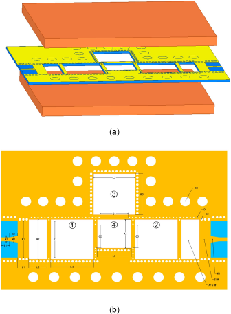
Figure 2. The simulation model of proposed filter: (a) structure of filter with NRN, (b) intermedia layer of filter with NRN (where M1 = 0.8 mm, M2 = 1.3 mm, B1 = 1.55 mm, B2 = 1.55 mm, W1 = 7.4 mm, W2 = 7.9 mm, W3 = 8.18 mm, G1 = 7.4 mm, G2 = 4.47 mm, G3 = 4.5 mm, G4 = 5.46 mm, L1 = 2.16 mm, L2 = 3.5 mm, L3 = 7.97 mm, L4 = 8.2 mm, L5 = 6.5 mm, A1 = 5.72 mm, D1 = 0.3 mm, D2 = 0.5 mm, and D3 = 2 mm).
In the simulation, these three layers are stacked together so that there is no gap between the adjacent layers to ensure the transmission of electromagnetic waves in the middle layer. Figure 2(b) shows the intermediate layer’s simulation model and dimensions, and the dimension unit is millimeters.
As shown in Fig. 2(b), the integrated transition structure composed of microstrip and SIW is used as the input and output ports of the AFSIW filter. This structure enables the AFSIW filter to be connected with a 2.92 mm RF coaxial connector, which facilitates S-parameter testing by the vector network. The transition structure will affect the filter’s cutoff frequency and return loss characteristics in the bandwidth. A good transition structure must be able to operate in a wide frequency band with a small insertion loss, and it can be machined in a relatively easy way. In this paper, two transition structures were fabricated in a back to back configuration. The transition structure mainly includes three parts: a 50 Ω microstrip line, a tapered transition microstrip, and a SIW cavity. Since the microstrip line transmits the Quasi-TEM mode wave while the SIW transmits the TE mode electromagnetic wave, the transition structure is required for the transmission mode conversion. This paper uses the tapered structure to transform the transmission mode between the 50 Ω microstrip line and the SIW cavity. The tapered transition structure is a linear gradient line, similar to that evolved from a step converter, where the number of steps gradually increases and the length of each step segment decreases. The characteristic impedance of the structure can smoothly transition from the characteristic impedance of one transmission line to another characteristic impedance, so it has good transition performance. The coupling between the resonant cavity and the NRN can be achieved by leaving a window between the air cavities. By adjusting the sizes of G1, G2, G3, and G4, the coupling strength between the cavities can be changed, thereby generating a TZ above the passband. Using HFSS to simulate the S-parameters, it can be seen from Fig. 3 that there is a TZ in the upper stopband of the AFSIW filter.
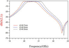
Figure 3. The curve of ![]() $\mathrm{S}_{21}$ against frequency for different L5 lengths with non-resonant node.
$\mathrm{S}_{21}$ against frequency for different L5 lengths with non-resonant node.
From the theory of NRN filter design, the bandwidth and the position of the TZ of the filter can be adjusted by changing the size of the NRN cavity [Reference Tomassoni, Silvestri, Ghiotto, Bozzi and Perregrini14]. As shown in Fig. 3, as the length of L5 decreases, the bandwidth of the filter gradually widens, and TZ moves slightly toward the high frequency. Under the premise of satisfying the passband flatness, the length of L5 can be adjusted appropriately to meet the actual requirements. It is known from Fig. 2(b) that the NRN is located in the transmission path of the AFSIW filter and connected to the resonant cavity. Modifying the size of the NRN will result in corresponding changes in both the resonant frequency of the cavity and the coupling coefficient with the NRN. Specifically, the resonant frequency of the cavity can be expressed using formula (1):
 \begin{equation}
f_{0}=\frac{c_{0}}{2\sqrt{\varepsilon _{r}}}\sqrt{\frac{1}{L_{e}^{2}}+\frac{1}{W_{e}^{2}}},
\end{equation}
\begin{equation}
f_{0}=\frac{c_{0}}{2\sqrt{\varepsilon _{r}}}\sqrt{\frac{1}{L_{e}^{2}}+\frac{1}{W_{e}^{2}}},
\end{equation}where
 \begin{equation}
L_{e}=L-\frac{D_{v}^{2}}{0.95P},\quad W_{e}=W-\frac{D_{v}^{2}}{0.95P},
\end{equation}
\begin{equation}
L_{e}=L-\frac{D_{v}^{2}}{0.95P},\quad W_{e}=W-\frac{D_{v}^{2}}{0.95P},
\end{equation}L and W, respectively, denote the effective length and width of the resonator. Additionally, Dv and P represent the diameter of the metallized via and the gap between adjacent vias, while c 0 and ɛr, respectively, refer to the speed of light in free space and the relative dielectric constant of the SIW dielectric substrate. As a result, a decrease in the length of L5 causes a shift of the center frequency toward higher frequencies.
In this study, we found that the transition air cavity between the input port and the AFSIW filter’s resonant cavity of the AFSIW filter also participates in the formation of the center frequency and TZ. Figure 4(a) shows the S-parameter simulation diagram of the shift of the center frequency and TZ of the AFSIW filter with the change of L2 when other parameters remain unchanged. The filter’s bandwidth remains almost unchanged, and the TZ and the center frequency move toward high frequencies as the length of L2 decreases. As shown in Fig. 4(b), as the length of W3 decreases, the TZ shifts toward higher frequencies, and the bandwidth increases slightly. This is because the change in W3 leads to a change in the size of the resonant cavity, which results in a change in the corresponding coupling coefficient and resonant frequency.
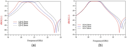
Figure 4. (a) The curve of ![]() $\mathrm{S}_{21}$ against frequency for different L2 lengths. (b) The curve of
$\mathrm{S}_{21}$ against frequency for different L2 lengths. (b) The curve of ![]() $\mathrm{S}_{21}$ against frequency for different W3 lengths.
$\mathrm{S}_{21}$ against frequency for different W3 lengths.
Fabrication and measurement results
A standard PCB process processes the AFSIW bandpass filter designed in this study. Figure 5(a) shows the intermediate layer circuit, and Fig. 5(b) shows the actual three-layer structure of the AFSIW filter. The intermediate layer circuit is made of Taconic TLY-5 dielectric material with a thickness of 0.508 mm, according to the model size in Fig. 2(b). In addition, through-holes with a diameter of 2.0 mm are added outside the resonant cavity of the intermediate layer circuit to fix the substrate, and through holes do not affect the microwave performance of the circuit. The upper and lower layers of the circuit are 1 mm thick silver-plated copper plates with a size of 27.5 mm× 37.02 mm. The diameter of the through holes in the upper and lower layers of the copper plate is 2.0 mm. Since the multi-layer board process is not used, M2 screws and nuts are used to fix the upper and lower copper plates and the middle layer circuit, as shown in Fig. 5(c). The width of the filter is 27.5 mm, the length is 43.22 mm, and the overall size is relatively small, so it is easy to integrate planar circuits. From the blue S 21 simulation curve in Fig. 5(d), it can be seen that the filter’s center frequency is 20.55 GHz, the bandwidth is 1.03 GHz, and its TZ is located at 22.74 GHz.
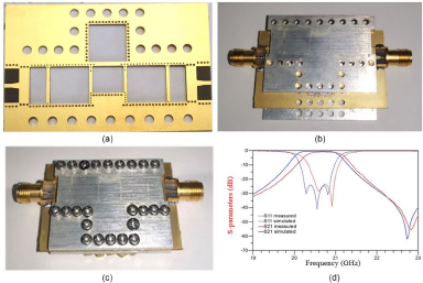
Figure 5. (a) Picture of middle layer circuit for the fabricated filter. (b) Picture of the actual three-layer structure for the fabricated filter. (c) Picture of assembly for the fabricated filter. (d) Measured and simulated S 21 and S 11 of the proposed filter.
The S-parameter were measured by a vector network analyzer whose calibration reference planes is the filter input–output coaxial port end face. The measurement results were compared with simulation results, as shown in Fig. 5(d). It can be seen from the figure that the measured in-band insertion loss is less than 0.95 dB, the bandwidth is 0.86 GHz, the center frequency is 20.73 GHz, and the relative bandwidth is 4.1% (3 dB bandwidth). The return loss is greater than 23 dB, indicating that the input and output ports are well matched. The deviation between the center frequency position and the simulation is about 180 MHz, caused by the PCB machining accuracy and the substrate assembly error [Reference Li, Ding, Wei and Wei Shi15]. It can be seen from the analysis in II that the position of the filter center frequency is very sensitive to the changes in the length of L5 and L2, so the deviation between the measured and simulated center frequencies is probably caused by the length errors of L5 and L2.
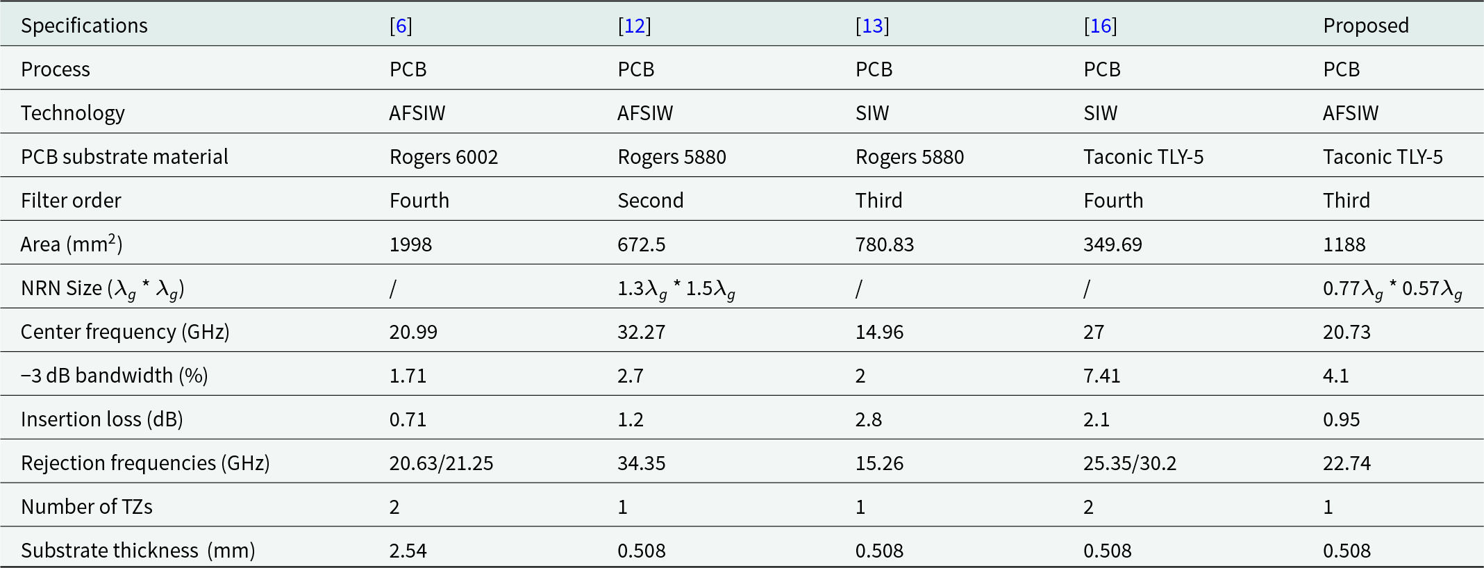
Table 1 summarizes the performance of bandpass filters using different techniques to compare to this study. The results show that the designed filter has good out-of-band rejection performance, and the NRN structure is miniaturized. Its insertion loss is lower than that of the SIW filter.
Table 1. Comparison with substrate integrated filters and air-filled substrate integrated filters
Conclusion
In this paper, an AFSIW bandpass filter for miniaturized NRN is designed and fabricated. Based on the existing AFSIW filter and NRN technology, this filter further reduces the size of NRN to have the advantage of miniaturization. It can be widely used in microwave and millimeter-wave fields. The introduction of NRN enables the filter to achieve a TZ above the passband to improve the filter selectivity. The miniaturization of NRN makes the filter size smaller. Moreover, by adjusting the size of the NRN cavity or the resonant cavity, the center frequency of the filter and the position of the TZ can be adjusted, which significantly improves the flexibility of the design.
Acknowledgements
This work was supported in part by the National Natural Science Foundation of China 12175176; the Chongqing Natural Science Foundation under Grant CSTB2022NSCQMSX1521; and the National Key Laboratory Foundation 6142411205202, 2021-JCJQ-LB-006.
Competing interests
The authors report no conflict of interest.

Yunlong Li was born in 2000, currently pursuing a master’s degree at the School of Aeronautics and Astronautics, University of Electronic Science and Technology of China. His main research interests include RF microwave circuit design and monolithic microwave integrated circuit.

Changjun Tian was born in 1997, currently pursuing a master’s degree at the School of Aeronautics and Astronautics, University of Electronic Science and Technology of China. His main research interests include RF microwave circuit design and microwave filters.

Shaozhuo Li was born in 1997, currently pursuing a master’s degree at the School of Aeronautics and Astronautics, University of Electronic Science and Technology of China. His main research interests include RF microwave circuit design and microwave filters.

Peng Chen received the B.S. degree in electronic science and technology and the Ph.D. degree in circuits and systems from the University of Electronic Science and Technology of China (UESTC), Chengdu, China, in 2009 and 2015, respectively. From 2015 to 2019, he was a Lecturer with the School of Aeronautics and Astronautics, UESTC. From 2017 to 2018, he was a Visiting Scholar supported by the China Scholarship Council (CSC), Tohoku University, Sendai, Japan, cooperated with Prof. Qiang Chen. Since 2019, he has been an Associate Professor with the School of Aeronautics and Astronautics, UESTC. He has authored or coauthored more than 20 papers in international journals and conferences. His current research interests include superconducting electronics, RF and microwave integrated circuits, and advanced electromagnetic communication systems.

Yun Li received the B.S. degree in telecommunication engineering and M.S. degree in electronics science and technology from Zhejiang University, Hangzhou, China, in 2008 and 2011, and the Ph.D. degree in electronics science and technology from Xi’an Jiaotong University, Xi’an, China in 2018. Since 2011, she has been an Engineer with the National Key Laboratory of Science and Technology on Space Microwave, China Academy of Space Technology, Xi’an, China, where she has been a Professor since 2021. Her current research interests include space microwave integration technology and space high-power microwave technology. She is the author of more than 60 articles, and more than 40 inventions. Prof Li is a recipient of the National “High-level Talents Program”. She also holds the outstanding young scholar reward from “Te Zhi Talents Program” in Shaanxi province.

Kai Yang received the B.S. degree in electronic science and technology and the master’s degree in circuits and systems from the University of Electronic Science and Technology of China (UESTC), Chengdu, China, in 1993 and 2000, respectively. In 2001, he was promoted as an Associate Professor with UESTC, where he was promoted as a Full Professor, in 2007. In 2002, he was selected as the Academic Outstanding Young Scientist Leader Training Plan of Sichuan Province. In 2003, he was a member of the National Superconducting Standardize Technology Committee. In 2006, he was selected as a Senior Member of the Chinese Institute of Electronics (CIE). He has authored or coauthored more than 50 papers in international and domestic journals and conferences. His current research interests include high-temperature superconducting circuits and systems, and RF and microwave passive circuits.


